Absolute maximum ratings, Operating ratings (notes , ), Package thermal resistance – Rainbow Electronics ADC08D1000 User Manual
Page 7: Converter electrical characteristics, Operating ratings
Absolute Maximum Ratings
(Notes 1, 2)
If Military/Aerospace specified devices are required,
please contact the National Semiconductor Sales Office/
Distributors for availability and specifications.
Supply Voltage (V
A
, V
DR
)
2.2V
Voltage on Any Input Pin
−0.15V to (V
A
+0.15V)
Ground Difference
|GND - DR GND|
0V to 100 mV
Input Current at Any Pin (Note 3)
±
25 mA
Package Input Current (Note 3)
±
50 mA
Power Dissipation at T
A
= 25˚C
2.0 W
ESD Susceptibility (Note 4)
Human Body Model
Machine Model
2500V
250V
Soldering Temperature, Infrared,
10 seconds (Note 5)
235˚C
Storage Temperature
−65˚C to +150˚C
Operating Ratings
(Notes 1, 2)
Ambient Temperature Range
−40˚C
≤ T
A
≤ +85˚C
Supply Voltage (V
A
)
+1.8V to +2.0V
Driver Supply Voltage (V
DR
)
+1.8V to V
A
Analog Input Common Mode
Voltage
1.2V to 1.3V
V
IN
Differential Voltage Range
−V
FS
/2 to +V
FS
/2
Ground Difference
(|GND - DR GND|)
0V
CLK Pins Voltage Range
0V to V
A
Differential CLK Amplitude
0.6V
P-P
to 2.0V
P-P
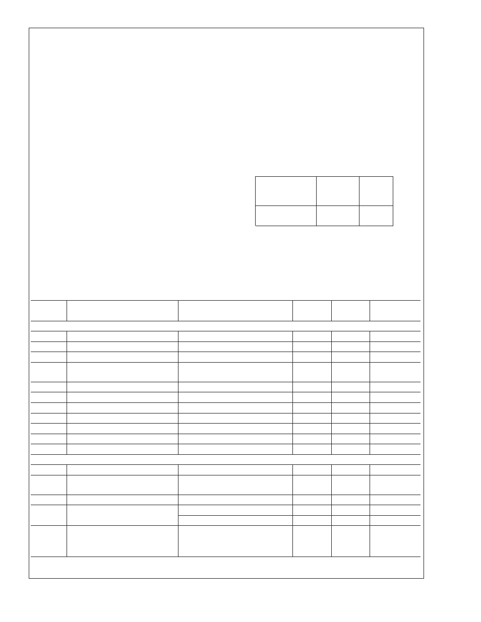
Package Thermal Resistance
Package
θ
JC
(Top of
Package)
θ
J-PAD
(Thermal
Pad)
128-Lead Exposed
Pad LQFP
10˚C / W
2.8˚C / W
Converter Electrical Characteristics
[Note: This product is currently in development. As such, the parameters specified in this section are DESIGN TAR-
GETS. The specifications in this section cannot be guaranteed until device characterization has taken place.]
The following specifications apply after calibration for V
A
= V
DR
= +1.9V
DC
, OutV = 1.9V, V
IN
FSR (a.c. coupled) = differential
860mV
P-P
, C
L
= 10 pF, Differential, a.c. coupled Sinewave Input Clock, f
CLK
= 1 GHz at 0.5V
P-P
with 50% duty cycle, Non-
Extended Control Mode, R
EXT
= 3300
Ω
±
0.1%, Analog Signal Source Impedance = 100
Ω. Boldface limits apply for T
A
=
T
MIN
to T
MAX
. All other limits T
A
= 25˚C, unless otherwise noted. (Notes 6, 7)
Symbol
Parameter
Conditions
Typical
Limits
Units
(Limits)
STATIC CONVERTER CHARACTERISTICS
INL
Integral Non-Linearity
±
0.35
±
TBD
LSB (max)
DNL
Differential Non-Linearity
±
0.25
±
TBD
LSB (max)
Resolution with No Missing Codes
8
Bits
V
OFF
Offset Error
-0.45
−TBD
TBD
LSB (min)
LSB (max)
V
OFF
_ADJ Input Offset Adjustment Range
Extended Control Mode
±
45
mV
TC V
OFF
Offset Error Tempco
−40˚C to +85˚C
−3
ppm/˚C
PFSE
Positive Full-Scale Error (Note 9)
−2.2
±
TBD
mV (max)
NFSE
Negative Full-Scale Error (Note 9)
−1.1
±
TBD
mV (max)
FS_ADJ
Full-Scale Adjustment Range
Extended Control Mode
±
20
±
15
%FS
TC PFSE
Positive Full-Scale Error Tempco
−40˚C to +85˚C
20
ppm/˚C
TC NFSE
Negative Full-Scale Error Tempco
−40˚C to +85˚C
13
ppm/˚C
Dynamic Converter Characteristics
FPBW
Full Power Bandwidth
Normal (non DES) Mode
1.7
GHz
FPBW
(DES)
Full Power Bandwidth
Dual Edge Sampling Mode
900
MHz
B.E.R.
Bit Error Rate
10
-18
Error/Bit
Gain Flatness
d.c. to 500 MHz
±
0.5
dBFS
d.c. to 1 GHz
±
1.0
dBFS
ENOB
Effective Number of Bits
f
IN
= 100 MHz, V
IN
= FSR − 0.5 dB
7.5
Bits
f
IN
= 248 MHz, V
IN
= FSR − 0.5 dB
7.5
TBD
Bits (min)
f
IN
= 498 MHz, V
IN
= FSR − 0.5 dB
7.5
TBD
Bits (min)
ADC08D1000
www.national.com
7