Note 3), Note 4), Note 5) – Rainbow Electronics ADC08D1000 User Manual
Page 11: Converter electrical characteristics
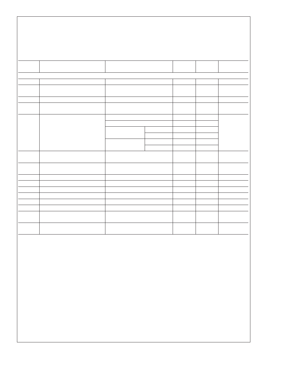
Converter Electrical Characteristics
(Continued)
[Note: This product is currently in development. As such, the parameters specified in this section are DESIGN TAR-
GETS. The specifications in this section cannot be guaranteed until device characterization has taken place.]
The following specifications apply after calibration for V
A
= V
DR
= +1.9V
DC
, OutV = 1.9V, V
IN
FSR (a.c. coupled) = differential
860mV
P-P
, C
L
= 10 pF, Differential, a.c. coupled Sinewave Input Clock, f
CLK
= 1 GHz at 0.5V
P-P
with 50% duty cycle, Non-
Extended Control Mode, R
EXT
= 3300
Ω
±
0.1%, Analog Signal Source Impedance = 100
Ω. Boldface limits apply for T
A
=
T
MIN
to T
MAX
. All other limits T
A
= 25˚C, unless otherwise noted. (Notes 6, 7)
Symbol
Parameter
Conditions
Typical
Limits
Units
(Limits)
AC ELECTRICAL CHARACTERISTICS
t
H
DCLK to Data Hold Time
DDR Mode, 180˚ DCLK (Note 12)
750
TBD
ps (min)
t
AD
Sampling (Aperture) Delay
Input CLK+ Fall to Acquisition of
Data
1.3
ns
t
AJ
Aperture Jitter
0.4
ps rms
t
OD
Input Clock to Data Output Delay
50% of Input Clock transition to
50% of Data transition
3.1
ns
Pipeline Delay (Latency)
DI Outputs
13
Input Clock
Cycles
DId Outputs
14
DQ Outputs
Normal Mode
13
DES Mode
13.5
DQd Outputs
Normal Mode
14
DES Mode
14.5
Over Range Recovery Time
Differential V
IN
step from
±
1.2V to
0V to get accurate conversion
TBD
ns
t
WU
PD low to Rated Accuracy
Conversion (Wake-Up Time)
500
ns
f
SCLK
Maximum Serial Clock Frequency
100
MHz
t
SSU
Data to Serial Clock Setup Time
2.5
TBD
ns (min)
t
SH
Data to Serial Clock Hold Time
1
TBD
ns (min)
Serial Clock Low Time
4
ns (min)
Serial Clock High Time
4
ns (min)
t
CAL
Calibration Cycle Time
1.4 x 10
5
Clock Cycles
t
CAL_L
CAL Pin Low Time
See Figure 9
80
Clock Cycles
(min)
t
CAL_H
CAL Pin High Time
See Figure 9
80
Clock Cycles
(min)
Note 1: Absolute Maximum Ratings indicate limits beyond which damage to the device may occur. There is no guarantee of operation at the Absolute Maximum
Ratings. Operating Ratings indicate conditions for which the device is functional, but do not guarantee specific performance limits. For guaranteed specifications and
test conditions, see the Electrical Characteristics. The guaranteed specifications apply only for the test conditions listed. Some performance characteristics may
degrade when the device is not operated under the listed test conditions.
Note 2: All voltages are measured with respect to GND = DR GND = 0V, unless otherwise specified.
Note 3: When the input voltage at any pin exceeds the power supply limits (that is, less than GND or greater than V
A
), the current at that pin should be limited to
25 mA. The 50 mA maximum package input current rating limits the number of pins that can safely exceed the power supplies with an input current of 25 mA to two.
This limit is not placed upon the power, ground and digital output pins.
Note 4: Human body model is 100 pF capacitor discharged through a 1.5 k
Ω resistor. Machine model is 220 pF discharged through ZERO Ohms.
Note 5: See AN-450, “Surface Mounting Methods and Their Effect on Product Reliability”.
Note 6: The analog inputs are protected as shown below. Input voltage magnitudes beyond the Absolute Maximum Ratings may damage this device.
ADC08D1000
www.national.com
11