2 out of range (or) indication, 3 full-scale input range, 3 the clock inputs – Rainbow Electronics ADC08D1000 User Manual
Page 26: 4 control pins, 1 full-scale input range setting, 2 self calibration, 1 power-on calibration, 0 applications information
2.0 Applications Information
(Continued)
2.2.2 Out Of Range (OR) Indication
When the conversion result is clipped the Out of Range
output is activated such that OR+ goes high and OR- goes
low. This output is active as long as accurate data on either
or both of the buses would be outside the range of 00h to
FFh.
2.2.3 Full-Scale Input Range
As with all A/D Converters, the input range is determined by
the value of the ADC’s reference voltage. The reference
voltage of the ADC08D1000 is derived from an internal
band-gap reference. The FSR pin controls the effective ref-
erence voltage of the ADC08D1000 such that the differential
full-scale input range at the analog inputs is 860 mV
P-P
with
the FSR pin high, or is 650 mV
P-P
with FSR pin low. Best
SNR is obtained with FSR high, but better distortion and
SFDR are obtained with the FSR pin low.
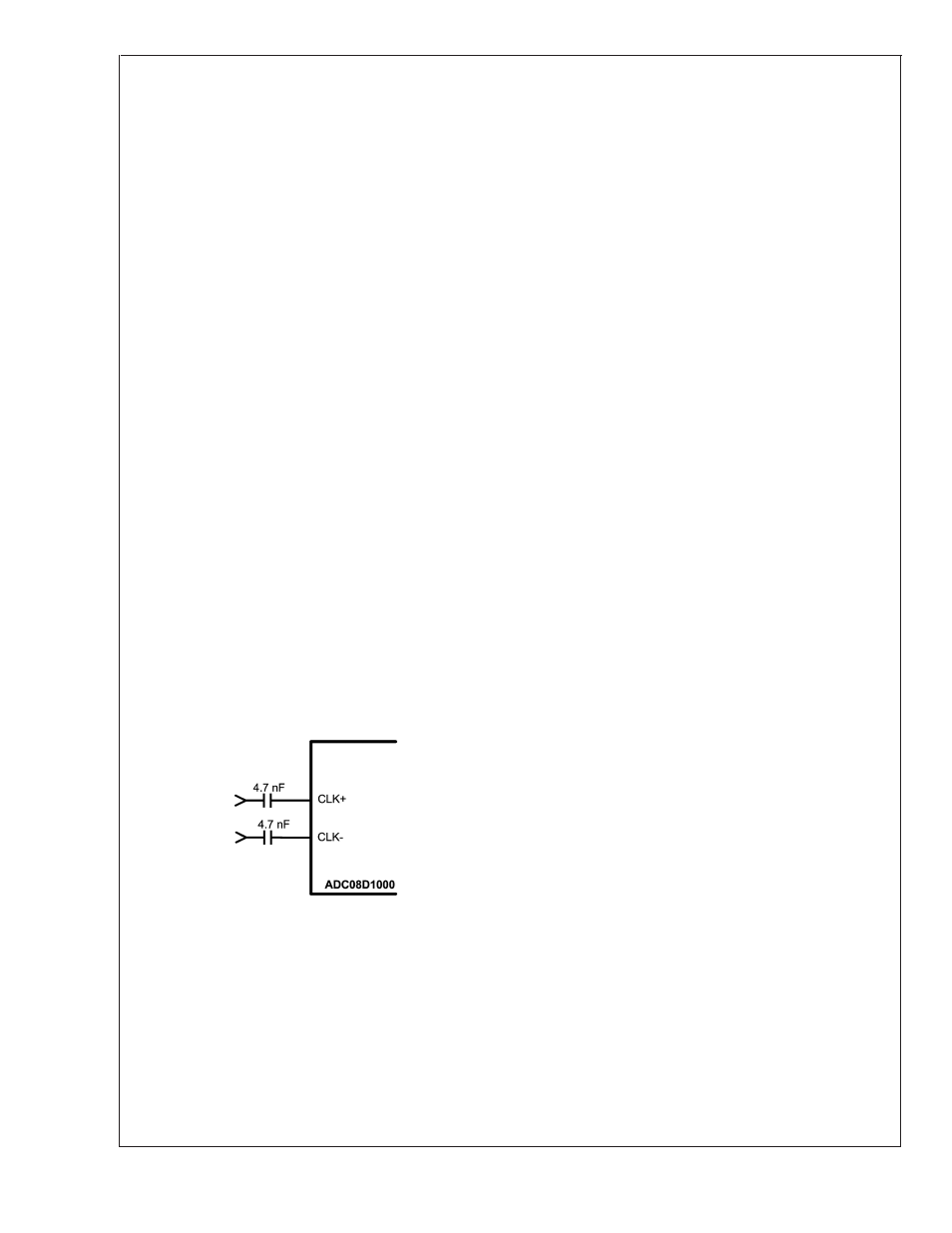
2.3 THE CLOCK INPUTS
The ADC08D1000 has differential LVDS clock inputs, CLK+
and CLK-, which must be driven with an a.c. coupled, differ-
ential clock signal. Although the ADC08D1000 is tested and
its performance is guaranteed with a differential 1.0 GHz
clock, it typically will function well with input clock frequen-
cies indicated in the Electrical Characteristics Table. The
clock inputs are internally terminated and biased. The input
clock signal must be capacitively coupled to the clock pins as
indicated in Figure 14.
Operation up to the sample rates indicated in the Electrical
Characteristics Table is typically possible if the maximum
ambient temperatures indicated are not exceeded. Operat-
ing at higher sample rates than indicated for the given am-
bient temperature may result in reduced device reliability
and product lifetime. This is because of the higher power
consumption and die temperatures at high sample rates.
Important also for reliability is proper thermal management .
See Section 2.6.2.
The differential input clock line pair should have a character-
istic impedance of 100
Ω and be terminated at the clock
source in that (100
Ω) characteristic impedance. The input
clock line should be as short and as direct as possible. The
ADC08D1000 clock input is internally terminated with an
untrimmed 100
Ω resistor.
Insufficient input clock levels will result in poor dynamic
performance. Excessively high input clock levels could
cause a change in the analog input offset voltage. To avoid
these problems, keep the input clock level within the range
specified in the Electrical Characteristics Table.
The low and high times of the input clock signal can affect
the performance of any A/D Converter. The ADC08D1000
features a duty cycle clock correction circuit which can main-
tain performance over temperature even in DES mode. The
ADC will meet its performance specification if the input clock
high and low times are maintained within the range (20/80%
ratio) as specified in the Electrical Characteristics Table.
High
speed,
high
performance
ADCs
such
as
the
ADC08D1000 require a very stable input clock signal with
minimum phase noise or jitter. ADC jitter requirements are
defined by the ADC resolution (number of bits), maximum
ADC input frequency and the input signal amplitude relative
to the ADC input full scale range. The maximum jitter (the
sum of the jitter from all sources) allowed to prevent a
jitter-induced reduction in SNR is found to be
t
J(MAX)
= (V
IN(P-P)
/V
INFSR
) x (1/(2
(N+1)
x
π x f
IN
))
where t
J(MAX)
is the rms total of all jitter sources in seconds,
V
IN(P-P)
is the peak-to-peak analog input signal, V
INFSR
is the
full-scale range of the ADC, "N" is the ADC resolution in bits
and f
IN
is the maximum input frequency, in Hertz, to the ADC
analog input.
Note that the maximum jitter described above is the arith-
metic sum of the jitter from all sources, including that in the
ADC input clock, that added by the system to the ADC input
clock and input signals and that added by the ADC itself.
Since the effective jitter added by the ADC is beyond user
control, the best the user can do is to keep the sum of the
externally added input clock jitter and the jitter added by the
analog circuitry to the analog signal to a minimum.
Input clock amplitudes above those specified in the Electrical
Characteristics Table may result in increased input offset
voltage. This would cause the converter to produce an out-
put code other than the expected 127/128 when both input
pins are at the same potential.
2.4 CONTROL PINS
Six control pins (without the use of the serial interface)
provide a wide range of possibilities in the operation of the
ADC08D1000 and facilitate its use. These control pins pro-
vide Full-Scale Input Range setting, Self Calibration, Calibra-
tion Delay, Output Edge Synchronization choice, LVDS Out-
put Level choice and a Power Down feature.
2.4.1 Full-Scale Input Range Setting
The input full-scale range can be selected to be either 650
mV
P-P
or 860 mV
P-P
, as selected with the FSR control input
(pin 14) in the Normal Mode of operation. In the Extended
Control Mode, the input full-scale range may be set to be
anywhere from 560 mV
P-P
to 840 mV
P-P
. See Section 2.2 for
more information.
2.4.2 Self Calibration
The ADC08D1000 self-calibration must be run to achieve
specified performance. The calibration procedure is run
upon power-up and can be run any time on command. The
calibration procedure is exactly the same whether there is an
input clock present upon power up or if the clock begins
some time after application of power. The CalRun output
indicator is high while a calibration is in progress.
2.4.2.1 Power-On Calibration
Power-on calibration begins after a time delay following the
application of power. This time delay is determined by the
setting of CalDly, as described in the Calibration Delay Sec-
tion, below.
20097447
FIGURE 14. Differential (LVDS) Input Clock Connection
ADC08D1000
www.national.com
26