Converter electrical characteristics – Rainbow Electronics ADC08D1000 User Manual
Page 10
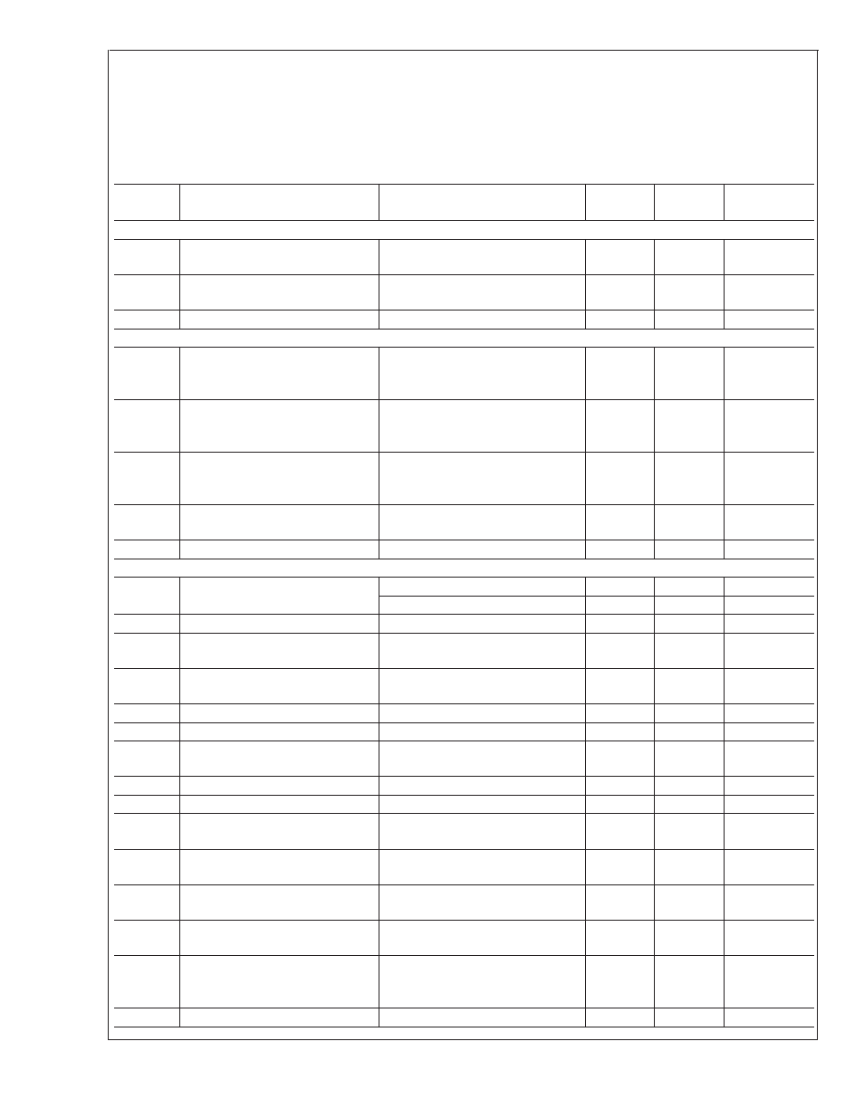
Converter Electrical Characteristics
(Continued)
[Note: This product is currently in development. As such, the parameters specified in this section are DESIGN TAR-
GETS. The specifications in this section cannot be guaranteed until device characterization has taken place.]
The following specifications apply after calibration for V
A
= V
DR
= +1.9V
DC
, OutV = 1.9V, V
IN
FSR (a.c. coupled) = differential
860mV
P-P
, C
L
= 10 pF, Differential, a.c. coupled Sinewave Input Clock, f
CLK
= 1 GHz at 0.5V
P-P
with 50% duty cycle, Non-
Extended Control Mode, R
EXT
= 3300
Ω
±
0.1%, Analog Signal Source Impedance = 100
Ω. Boldface limits apply for T
A
=
T
MIN
to T
MAX
. All other limits T
A
= 25˚C, unless otherwise noted. (Notes 6, 7)
Symbol
Parameter
Conditions
Typical
Limits
Units
(Limits)
DIGITAL OUTPUT CHARACTERISTICS
∆ V
OS
Output Offset Voltage Change
Between Logic Levels
±
1
mV
I
OS
Output Short Circuit Current
Output+ & Output- connected to
0.8V
±
4
mA
Z
O
Differential Output Impedance
100
Ohms
POWER SUPPLY CHARACTERISTICS
I
A
Analog Supply Current
PD = PDQ = Low
PD = Low, PDQ = High
PD = High
627
325
4.3
690
360
mA (max)
mA
mA
I
DR
Output Driver Supply Current
PD = PDQ = Low
PD = Low, PDQ = High
PD = PDQ = High
202
116
1
257
135
mA (max)
mA (max)
mA
P
D
Power Consumption
PD = PDQ = Low
PD = Low, PDQ = High
PD = PDQ = High
1.6
0.84
20
1.8
0.94
W (max)
W
mW
PSRR1
D.C. Power Supply Rejection Ratio
Change in Full Scale Error with
change in V
A
from 1.8V to 2.0V
73
dB
PSRR2
A.C. Power Supply Rejection Ratio
248 MHz, 50mV
P-P
riding on V
A
TBD
dB
AC ELECTRICAL CHARACTERISTICS
f
CLK1
Maximum Conversion Rate
T
A
≤ 85˚C
1.1
1.0
GHz (min)
T
A
≤ 75˚C
1.3
GHz
f
CLK2
Minimum Conversion Rate
200
MHz
Input Clock Duty Cycle
200 MHz
≤ Input clock frequency ≤
1 GHz (Normal Mode)
50
20
80
% (min)
% (max)
Input Clock Duty Cycle
500MHz
≤ Input clock frequency ≤ 1
GHz (DES Mode)
50
20
80
% (min)
% (max)
t
CL
Input Clock Low Time
500
200
ps (min)
t
CH
Input Clock High Time
500
200
ps (min)
DCLK Duty Cycle
50
45
55
% (min)
% (max)
t
RS
Reset Setup Time
150
TBD
ps (min)
t
RH
Reset Hold Time
250
TBD
ps (min)
t
SD
Syncronizing Edge to DCLK Output
Delay
f
CLKIN
= 1.0 GHz
f
CLKIN
= 200 MHz
3.53
3.85
ns
t
RPW
Reset Pulse Width
4
Clock Cycles
(min)
t
LHT
Differential Low to High Transition
Time
10% to 90%, C
L
= 2.5 pF
250
ps
t
HLT
Differential High to Low Transition
Time
10% to 90%, C
L
= 2.5 pF
250
ps
t
OSK
DCLK to Data Output Skew
50% of DCLK transition to 50% of
Data transition, SDR Mode
and DDR Mode, 0˚ DCLK (Note 12)
±
50
±
200
ps (max)
t
SU
Data to DCLK Set-Up Time
DDR Mode, 180˚ DCLK (Note 12)
750
TBD
ps (min)
ADC08D1000
www.national.com
10