6 power down feature, 5 the digital outputs, 6 power considerations – Rainbow Electronics ADC08D1000 User Manual
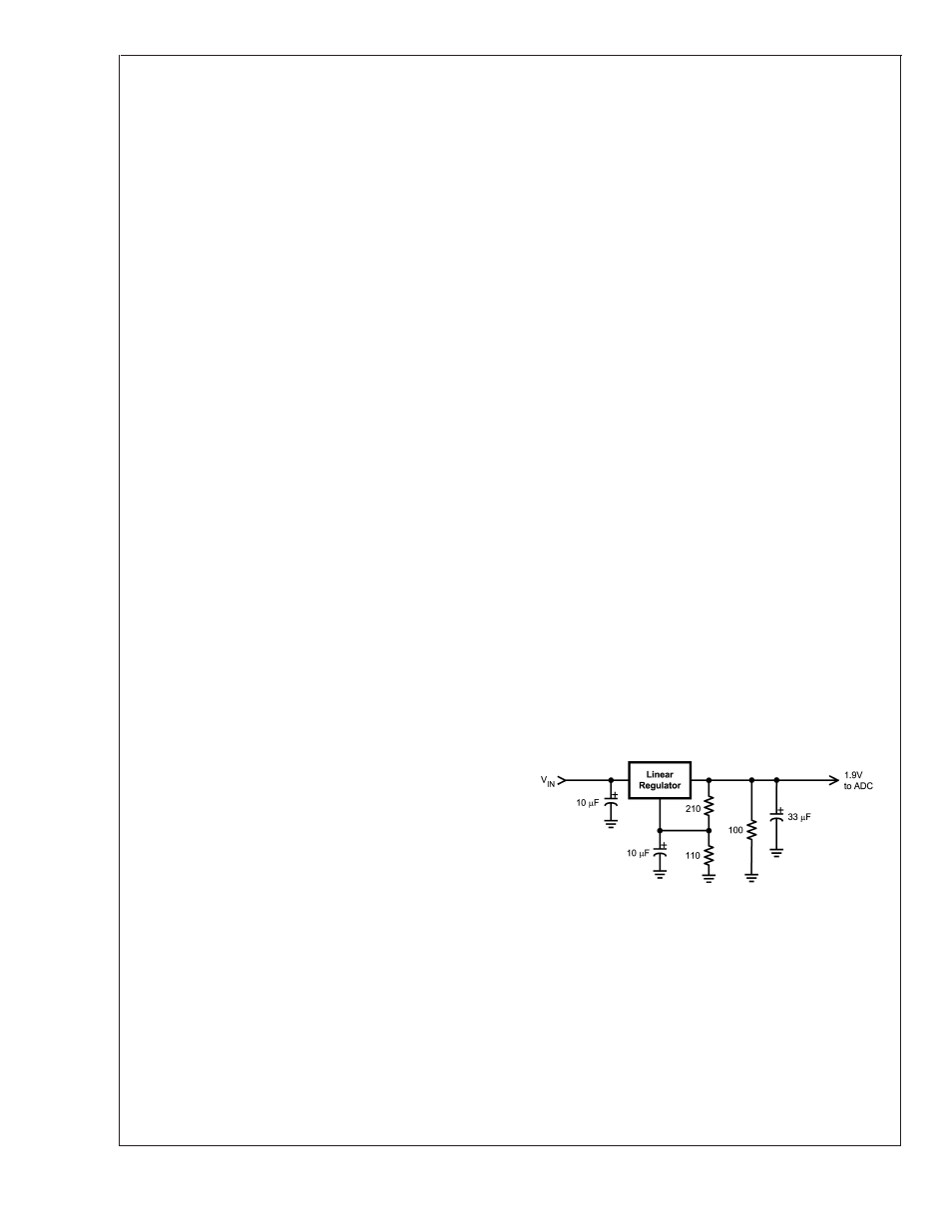
Page 28: 1 supply voltage, Figure 15. non-spiking power supply, 0 applications information
2.0 Applications Information
(Continued)
2.4.6 Power Down Feature
The
Power
Down
pins
(PD
and
PDQ)
allow
the
ADC08D1000 to be entirely powered down (PD) or the "Q"
channel to be powered down and the "I" channel to remain
active. See Section 1.1.7 for details on the power down
feature.
The digital data (+/-) output pins are put into a high imped-
ance state when the PD pin for the respective channel is
high. Upon return to normal operation, the pipeline will con-
tain meaningless information and must be flushed.
If the PD input is brought high while a calibration is running,
the device will not go into power down until the calibration
sequence is complete. However, if power is applied and PD
is already high, the device will not begin the calibration
sequence until the PD input goes low. If a manual calibration
is requested while the device is powered down, the calibra-
tion will not begin at all. That is, the manual calibration input
is completely ignored in the power down state.
2.5 THE DIGITAL OUTPUTS
The ADC08D1000 demultiplexes the output data of each of
the two ADCs on the die onto two LVDS output buses (total
of four buses, two for each ADC). For each of the two
converters, the results of successive conversions started on
the odd falling edges of the CLK+ pin are available on one of
the two LVDS buses, while the results of conversions started
on the even falling edges of the CLK+ pin are available on
the other LVDS bus. This means that, the word rate at each
LVDS bus is 1/2 the ADC08D1000 input clock rate and the
two buses must be multiplexed to obtain the entire 1 GSPS
conversion result.
Since the minimum recommended input clock rate for this
device is 200 MSPS, the effective rate can be reduced to as
low as 100 MSPS by using the results available on just one
of the the two LVDS buses and a 200 MHz input clock,
decimating the 200 MSPS data by two.
There is one LVDS output clock pair (DCLK) available for
use to latch the LVDS outputs on all buses. Whether the data
is sent at the rising or falling edge of DCLK is determined by
the sense of the OutEdge pin, as described in Section 2.4.3.
DDR (Double Data Rate) clocking can also be used. In this
mode a word of data is presented with each edge of DCLK,
reducing the DCLK frequency to 1/4 the input clock fre-
quency. See the Timing Diagram section for details.
The OutV pin is used to set the LVDS differential output
levels. See Section 2.4.4.
The output format is Offset Binary. Accordingly, a full-scale
input level with V
IN
+ positive with respect to V
IN
− will pro-
duce an output code of all ones, a full-scale input level with
V
IN
− positive with respect to V
IN
+ will produce an output
code of all zeros and when V
IN
+ and V
IN
− are equal, the
output code will vary between codes 127 and 128.
2.6 POWER CONSIDERATIONS
A/D converters draw sufficient transient current to corrupt
their own power supplies if not adequately bypassed. A 33
µF capacitor should be placed within an inch (2.5 cm) of the
A/D converter power pins. A 0.1 µF capacitor should be
placed as close as possible to each V
A
pin, preferably within
one-half centimeter. Leadless chip capacitors are preferred
because they have low lead inductance.
The V
A
and V
DR
supply pins should be isolated from each
other to prevent any digital noise from being coupled into the
analog portions of the ADC. A ferrite choke, such as the JW
Miller FB20009-3B, is recommended between these supply
lines when a common source is used for them.
As is the case with all high speed converters, the
ADC08D1000 should be assumed to have little power supply
noise rejection. Any power supply used for digital circuitry in
a system where a lot of digital power is being consumed
should not be used to supply power to the ADC08D1000.
The ADC supplies should be the same supply used for other
analog circuitry, if not a dedicated supply.
2.6.1 Supply Voltage
The ADC08D1000 is specified to operate with a supply
voltage of 1.9V
±
0.1V. It is very important to note that, while
this device will function with slightly higher supply voltages,
these higher supply voltages may reduce product lifetime.
No pin should ever have a voltage on it that is in excess of
the supply voltage or below ground by more than 150 mV,
not even on a transient basis. This can be a problem upon
application of power and power shut-down. Be sure that the
supplies to circuits driving any of the input pins, analog or
digital, do not come up any faster than does the voltage at
the ADC08D1000 power pins.
The Absolute Maximum Ratings should be strictly observed,
even during power up and power down. A power supply that
produces a voltage spike at turn-on and/or turn-off of power
can destroy the ADC08D1000. The circuit of Figure 15 will
provide supply overshoot protection.
Many linear regulators will produce output spiking at
power-on unless there is a minimum load provided. Active
devices draw very little current until their supply voltages
reach a few hundred millivolts. The result can be a turn-on
spike that can destroy the ADC08D1000, unless a minimum
load is provided for the supply. The 100
Ω resistor at the
regulator output provides a minimum output current during
power-up to ensure there is no turn-on spiking.
In the circuit of Figure 15, an LM317 linear regulator is
satisfactory if its input supply voltage is 4V to 5V . If a 3.3V
supply is used, an LM1086 linear regulator is recommended.
The output drivers should have a supply voltage, V
DR
, that is
within the range specified in the Operating Ratings table.
This voltage should not exceed the V
A
supply voltage.
If the power is applied to the device without an input clock
signal present, the current drawn by the device might be
below 200 mA. This is because the ADC08D1000 gets reset
through clocked logic and its initial state is random. If the
reset logic comes up in the "on" state, it will cause most of
the analog circuitry to be powered down, resulting in less
than 100 mA of current draw. This current is greater than the
20097454
FIGURE 15. Non-Spiking Power Supply
ADC08D1000
www.national.com
28