Pin descriptions and equivalent circuits – Rainbow Electronics ADC08D1000 User Manual
Page 4
Pin Descriptions and Equivalent Circuits
(Continued)
Pin Functions
Pin No.
Symbol
Equivalent Circuit
Description
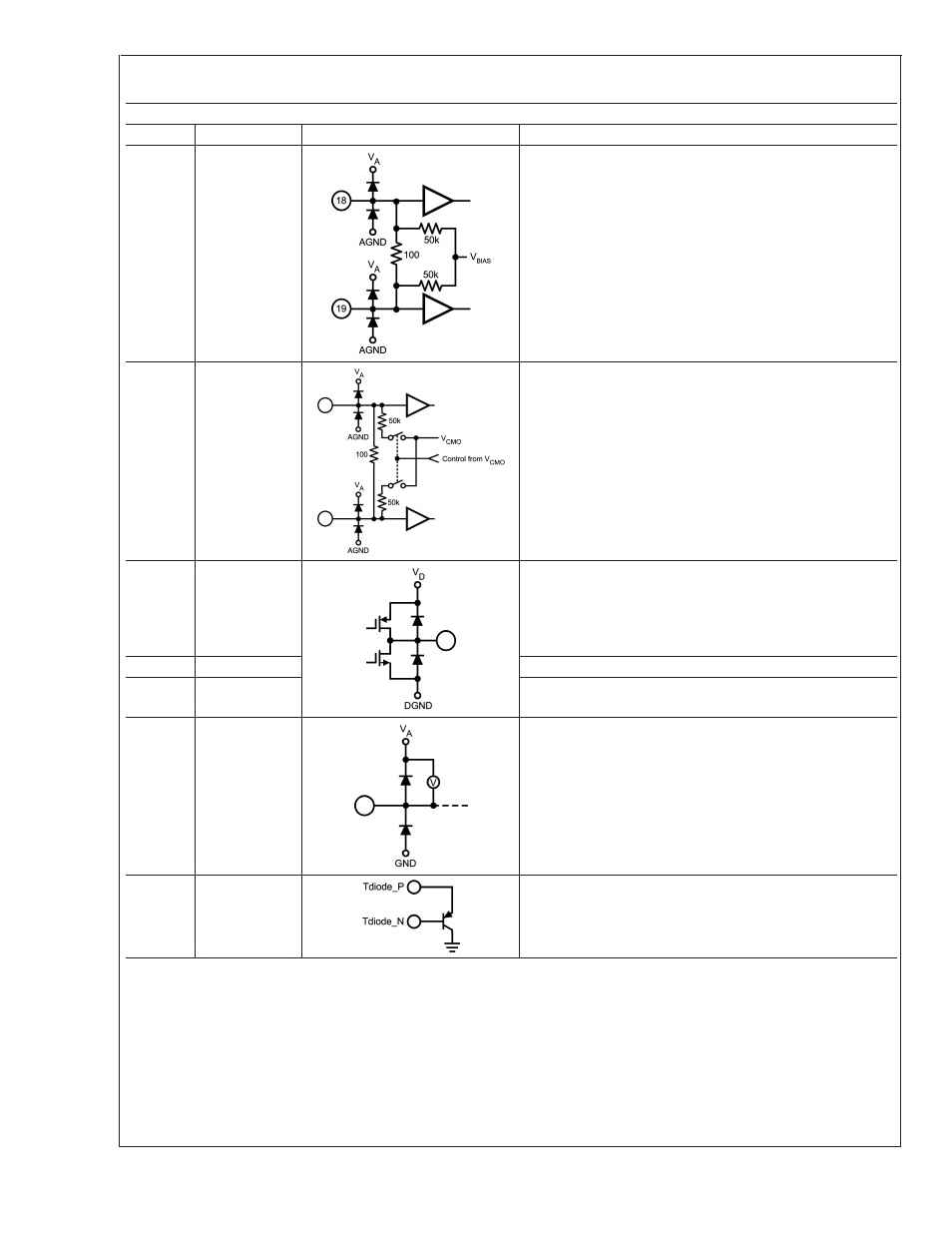
18
19
CLK+
CLK-
LVDS Clock input pins for the ADC. The differential clock
signal must be a.c. coupled to these pins. The input signal is
sampled on the falling edge of CLK+. See Section 2.3.
11
10
.
22
23
V
IN
I+
V
IN
I−
.
V
IN
Q+
V
IN
Q−
Analog signal inputs to the ADC. The differential full-scale
input range is 650 mV
P-P
when the FSR pin is low, or 860
mV
P-P
when the FSR pin is high.
7
V
CMO
Common Mode Voltage. The voltage output at this pin is
required to be the common mode input voltage at V
IN
+ and
V
IN
− when d.c. coupling is used. This pin should be grounded
when a.c. coupling is used at the analog inputs. This pin is
capable of sourcing or sinking 100µA. See Section 2.2.
31
V
BG
Bandgap output voltage capable of 100 µA source/sink.
126
CalRun
Calibration Running indication. This pin is at a logic high when
calibration is running.
32
R
EXT
External bias resistor connection. Nominal value is 3.3k-Ohms
(
±
0.1%) to ground. See Section 1.1.1.
34
35
Tdiode_P
Tdiode_N
Temperature Diode Positive (Anode) and Negative (Cathode)
for die temperature measurements. See Section 2.6.2.
ADC08D1000
www.national.com
4