2 thermal management, Figure 16. recommended package land pattern, 7 layout and grounding – Rainbow Electronics ADC08D1000 User Manual
Page 29: 0 applications information
2.0 Applications Information
(Continued)
power down current because not all of the ADC is powered
down. The device current will be normal after the input clock
is established.
2.6.2 Thermal Management
The ADC08D1000 is capable of impressive speeds and
performance at very low power levels for its speed. However,
the power consumption is still high enough to require atten-
tion to thermal management. For reliability reasons, the die
temperature should be kept to a maximum of 130˚C. That is,
t
A
(ambient temperature) plus ADC power consumption
times
θ
JA
(junction to ambient thermal resistance) should not
exceed 130˚C. This is not a problem if the ambient tempera-
ture is kept to a maximum of +85˚C with the requisite amount
of airflow as specified in the Operating Ratings section.
Please note that the following are general recommendations
for mounting exposed pad devices onto a PCB. This should
be considered the starting point in PCB and assembly pro-
cess development. It is recommended that the process be
developed based upon past experience in package mount-
ing.
The package of the ADC08D1000 has an exposed pad on its
back that provides the primary heat removal path as well as
excellent electrical grounding to the printed circuit board.
The land pattern design for lead attachment to the PCB
should be the same as for a conventional LQFP, but the
exposed pad must be attached to the board to remove the
maximum amount of heat from the package, as well as to
ensure best product parametric performance.
To maximize the removal of heat from the package, a ther-
mal land pattern must be incorporated on the PC board
within the footprint of the package. The exposed pad of the
device must be soldered down to ensure adequate heat
conduction out of the package. The land pattern for this
exposed pad should be at least as large as the 5 x 5 mm of
the exposed pad of the package and be located such that the
exposed pad of the device is entirely over that thermal land
pattern. This thermal land pattern should be electrically con-
nected to ground. A clearance of at least 0.5 mm should
separate this land pattern from the mounting pads for the
package pins.
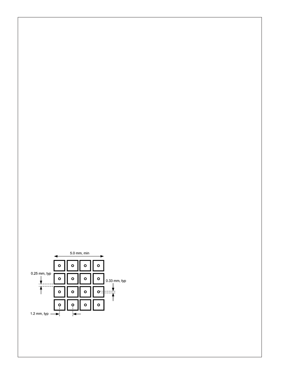
Since a large aperture opening may result in poor release,
the aperture opening should be subdivided into an array of
smaller openings, similar to the land pattern of Figure 16.
To minimize junction temperature, it is recommended that a
simple heat sink be built into the PCB. This is done by
including a copper area of about 2 square inches (6.5 square
cm) on the opposite side of the PCB. This copper area may
be plated or solder coated to prevent corrosion, but should
not have a conformal coating, which could provide some
thermal insulation. Thermal vias should be used to connect
these top and bottom copper areas. These thermal vias act
as "heat pipes" to carry the thermal energy from the device
side of the board to the opposite side of the board where it
can be more effectively dissipated. The use of 9 to 16
thermal vias is recommended.
The thermal vias should be placed on a 1.2 mm grid spacing
and have a diameter of 0.30 to 0.33 mm. These vias should
be barrel plated to avoid solder wicking into the vias during
the soldering process as this wicking could cause voids in
the solder between the package exposed pad and the ther-
mal land on the PCB. Such voids could increase the thermal
resistance between the device and the thermal land on the
board, which would cause the device to run hotter.
If it is desired to monitor die temperature, a temperature
sensor may be mounted on the heat sink area of the board
near the thermal vias. .Allow for a thermal gradient between
the temperature sensor and the ADC08D1000 die of
θ
Jc
times typical power consumption = 2.8 x 1.6 = 4.5˚C. Allow-
ing for a 5.5˚C (including an extra 1˚C) temperature drop
from the die to the temperature sensor, then, would mean
that maintaining a maximum pad temperature reading of
124.5˚C will ensure that the die temperature does not ex-
ceed 130˚C, assuming that the exposed pad of the
ADC08D1000 is properly soldered down and the thermal
vias are adequate. (The inaccuracy of the temperature sen-
sor is addtional to the above calculation).
2.7 LAYOUT AND GROUNDING
Proper grounding and proper routing of all signals are es-
sential to ensure accurate conversion. A single ground plane
should be used, as apposed to splitting the ground plane into
analog and digital areas.
Since digital switching transients are composed largely of
high frequency components, the skin effect tells us that total
ground plane copper weight will have little effect upon the
logic-generated noise. Total surface area is more important
than is total ground plane volume. Coupling between the
typically noisy digital circuitry and the sensitive analog cir-
cuitry can lead to poor performance that may seem impos-
sible to isolate and remedy. The solution is to keep the
analog circuitry well separated from the digital circuitry.
High power digital components should not be located on or
near any linear component or power supply trace or plane
that services analog or mixed signal components as the
resulting common return current path could cause fluctuation
in the analog input “ground” return of the ADC, causing
excessive noise in the conversion result.
Generally, we assume that analog and digital lines should
cross each other at 90˚ to avoid getting digital noise into the
analog path. In high frequency systems, however, avoid
crossing analog and digital lines altogether. The input clock
lines should be isolated from ALL other lines, analog AND
digital. The generally accepted 90˚ crossing should be
avoided as even a little coupling can cause problems at high
frequencies. Best performance at high frequencies is ob-
tained with a straight signal path.
The analog input should be isolated from noisy signal traces
to avoid coupling of spurious signals into the input. This is
especially important with the low level drive required of the
20097421
FIGURE 16. Recommended Package Land Pattern
ADC08D1000
www.national.com
29