8 dynamic performance, 9 using the serial interface, 1 non-extended control mode operation – Rainbow Electronics ADC08D1000 User Manual
Page 30: 10 common application pitfalls, 0 applications information
2.0 Applications Information
(Continued)
ADC08D1000. Any external component (e.g., a filter capaci-
tor) connected between the converter’s input and ground
should be connected to a very clean point in the analog
ground plane. All analog circuitry (input amplifiers, filters,
etc.) should be separated from any digital components.
2.8 DYNAMIC PERFORMANCE
The ADC08D1000 is a.c. tested and its dynamic perfor-
mance is guaranteed. To meet the published specifications
and avoid jitter-induced noise, the clock source driving the
CLK input must exhibit low rms jitter. The allowable jitter is a
function of the input frequency and the input signal level, as
described in Section 2.3.
It is good practice to keep the ADC input clock line as short
as possible, to keep it well away from any other signals and
to treat it as a transmission line. Other signals can introduce
jitter into the input clock signal. The clock signal can also
introduce noise into the analog path if not isolated from that
path.
Best dynamic performance is obtained when the exposed
pad at the back of the package has a good connection to
ground. This is because this path from the die to ground is a
lower impedance than offered by the package pins.
2.9 USING THE SERIAL INTERFACE
The ADC08D1000 may be operated in the non-extended
control (non-Serial Interface) mode or in the extended con-
trol mode. Table 6 and Table 7 describe the functions of pins
3, 4, 14 and 127 in the non-extended control mode and the
extended control mode, respectively.
2.9.1 Non-Extended Control Mode Operation
Non-extended control mode operation means that the Serial
Interface is not active and all controllable functions are con-
trolled with various pin settings. That is, the full-scale range,
single-ended or differential input and input coupling (a.c. or
d.c.) are all controlled with pin settings. The non-extended
control mode is used by setting pin 14 high or low, as
opposed to letting it float. Table 6 indicates the pin functions
of the ADC08D1000 in the non-extended control mode.
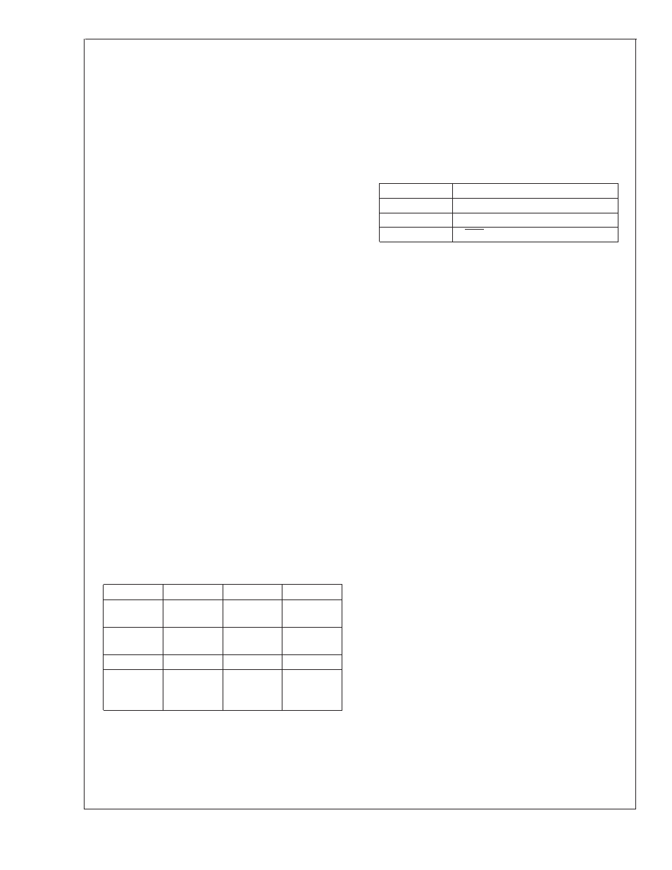
TABLE 6. Non-Extended Control Mode Operation (Pin
14 High or Low)
Pin
Low
High
Floating
3
0.44V
P-P
Output
0.6V
P-P
Output
n/a
4
OutEdge =
Neg
OutEdge =
Pos
DDR
127
CalDly Low
CalDly High
DES
14
650 mV
P-P
input range
860 mV
P-P
input range
Extended
Control
Mode
Pin 3 can be either high or low in the non-extended control
mode. Pin 14 must not be left floating to select this mode.
See Section 1.2 for more information.
Pin 4 can be high or low or can be left floating in the
non-extended control mode. In the non-extended control
mode, pin 4 high or low defines the edge at which the output
data transitions. See Section 2.4.3 for more information. If
this pin is floating, the output clock (DCLK) is a DDR (Double
Data Rate) clock (see Section 1.1.5.3) and the output edge
synchronization is irrelevant since data is clocked out on
both DCLK edges.
Pin 127, if it is high or low in the non-extended control mode,
sets the calibration delay. If pin 127 is floating, the calibration
delay is the same as it would be with this pin low and the
converter performs dual edge sampling (DES).
TABLE 7. Extended Control Mode Operation (Pin 14
Floating)
Pin
Function
3
SCLK (Serial Clock)
4
SDATA (Serial Data)
127
SCS (Serial Interface Chip Select)
2.10 COMMON APPLICATION PITFALLS
Driving the inputs (analog or digital) beyond the power
supply rails. For device reliability, no input should go more
than 150 mV below the ground pins or 150 mV above the
supply pins. Exceeding these limits on even a transient basis
may not only cause faulty or erratic operation, but may
impair device reliability. It is not uncommon for high speed
digital circuits to exhibit undershoot that goes more than a
volt below ground. Controlling the impedance of high speed
lines and terminating these lines in their characteristic im-
pedance should control overshoot.
Care should be taken not to overdrive the inputs of the
ADC08D1000. Such practice may lead to conversion inac-
curacies and even to device damage.
Incorrect analog input common mode voltage in the d.c.
coupled mode. As discussed in section 1.3 and 3.0, the Input
common mode voltage must remain within 50 mV of the
V
CMO
output , which has a variability with temperature that
must also be tracked. Distortion performance will be de-
graded if the input common mode voltages more than 50 mV
from V
CMO
.
Using an inadequate amplifier to drive the analog input.
Use care when choosing a high frequency amplifier to drive
the ADC08D1000 as many high speed amplifiers will have
higher distortion than will the ADC08D1000, resulting in
overall system performance degradation.
Driving the V
BG
pin to change the reference voltage. As
mentioned in Section 2.1, the reference voltage is intended
to be fixed to provide one of two different full-scale values
(650 mV
P-P
and 860 mV
P-P
). Over driving this pin will not
change the full scale value, but can otherwise upset opera-
tion.
Driving the clock input with an excessively high level
signal. The ADC input clock level should not exceed the
level described in the Operating Ratings Table or the input
offset could change.
Inadequate input clock levels. As described in Section 2.3,
insufficient input clock levels can result in poor performance.
Excessive input clock levels could result in the introduction
of an input offset.
Using a clock source with excessive jitter, using an
excessively long input clock signal trace, or having
other signals coupled to the input clock signal trace.
This will cause the sampling interval to vary, causing exces-
sive output noise and a reduction in SNR performance.
ADC08D1000
www.national.com
30