3 the serial interface, Table 4. register addresses, 4 register description – Rainbow Electronics ADC08D1000 User Manual
Page 21: Configuration register, 0 functional description
1.0 Functional Description
(Continued)
The default state of the Extended Control Mode is set upon
power-on reset (internally performed by the device) and is
shown in Table 3.
TABLE 3. Extended Control Mode Operation (Pin 14
Floating)
Feature
Extended Control Mode
Default State
SDR or DDR Clocking
DDR Clocking
DDR Clock Phase
Data changes with DCLK
edge (0˚ phase)
LVDS Output Amplitude
Normal amplitude
(600 mV
P-P
)
Calibration Delay
Short Delay
Full-Scale Range
700 mV nominal for both
channels
Input Offset Adjust
No adjustment for either
channel
Dual Edge Sampling
(DES)
Not enabled
1.3 THE SERIAL INTERFACE
The 3-pin serial interface is enabled only when the device is
in the Extended Control mode. The pins of this interface are
Serial Clock (SCLK), Serial Data (SDATA) and Serial Inter-
face Chip Select (SCS) Eight write only registers are acces-
sible through this serial interface.
SCS: This signal should be asserted low while accessing a
register through the serial interface. Setup and hold times
with respect to the SCLK must be observed.
SCLK: Serial data input is accepted with the rising edge of
this signal.
SDATA: Each register access requires a specific 32-bit pat-
tern at this input. This pattern consists of a header, register
address and register value. The data is shifted in MSB first.
Setup and hold times with respect to the SCLK must be
observed. See the Timing Diagram.
Each Register access consists of 32 bits, as shown in Figure
5 of the Timing Diagrams. The fixed header pattern is 0000
0000 0001 (eleven zeros followed by a 1). The loading
sequence is such that a "0" is loaded first. These 12 bits form
the header. The next 4 bits are the address of the register
that is to be written to and the last 16 bits are the data written
to the addressed register. The addresses of the various
registers are indicated in Table 4.
Refer to the Register Description (Section 1.4) for informa-
tion on the data to be written to the registers.
Subsequent register accesses may be performed immedi-
ately, starting with the 33rd SCLK. This means that the SCS
input does not have to be deasserted and asserted again
between register addresses. It is possible, although not rec-
ommended, to keep the SCS input permanently enabled (at
a logic low) when using extended control.
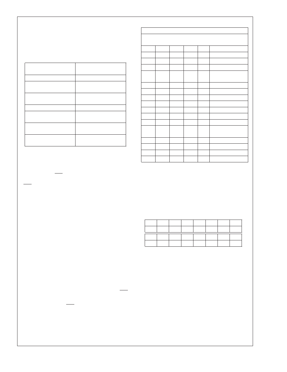
TABLE 4. Register Addresses
4-Bit Address
Loading Sequence:
A3 loaded after H0, A0 loaded last
A3
A2
A1
A0
Hex
Register Addressed
0
0
0
0
0h
Reserved
0
0
0
1
1h
Configuration
0
0
1
0
2h
"I" Ch Offset
0
0
1
1
3h
"I" Ch Full-Scale
Voltage Adjust
0
1
0
0
4h
Reserved
0
1
0
1
5h
Reserved
0
1
1
0
6h
Reserved
0
1
1
1
7h
Reserved
1
0
0
0
8h
Reserved
1
0
0
1
9h
Reserved
1
0
1
0
Ah
"Q" Ch Offset
1
0
1
1
Bh
"Q" Ch Full-Scale
Voltage Adjust
1
1
0
0
Ch
Reserved
1
1
0
1
Dh
DES Enable
1
1
1
0
Eh
DES Coarse Adjust
1
1
1
1
Fh
DES Fine Adjust
1.4 REGISTER DESCRIPTION
Eight write-only registers provide several control and con-
figuration options in the Extended Control Mode. These reg-
isters have no effect when the device is in the Normal
Control Mode. Each register description below also shows
the Power-On Reset (POR) state of each control bit.
Configuration Register
Addr: 1h (0001b)
W only (0xB2FF)
D15
D14
D13
D12
D11
D10
D9
D8
1
0
1
DCS
DCP
nDE
OV
OE
D7
D6
D5
D4
D3
D2
D1
D0
1
1
1
1
1
1
1
1
Bit 15
Must be set to 1b
Bit 14
Must be set to 0b
Bit 13
Must be set to 1b
Bit 12
DCS:Duty Cycle Stabilizer. When this bit is
set to 1b , a duty cycle stabilzation circuit is
applied to the clock input. When this bit is set
to 0b the stabilzation circuit is disabled.
POR State: 1b
Bit 11
DCP: DDR Clock Phase. This bit only has an
effect in the DDR mode. When this bit is set
to 0b, the DCLK edges are time-aligned with
the data bus edges ("0˚ Phase"). When this
bit is set to a 1b, the DCLK edges are placed
in the middle of the data bit-cells ("180˚
Phase").
POR State: 0b
ADC08D1000
www.national.com
21