Rainbow Electronics ADC08D1000 User Manual
General description, Features, Key specifications
ADC08D1000
High Performance, Low Power, Dual 8-Bit, 1 GSPS A/D
Converter
General Description
NOTE: This product is currently in development. – ALL
specifications are design targets and are subject to
change.
The ADC08D1000 is a dual, low power, high performance
CMOS analog-to-digital converter that digitizes signals to 8
bits resolution at sampling rates up to 1.3 GSPS. Consuming
a typical 1.6 Watts at 1 GSPS from a single 1.9 Volt supply,
this device is guaranteed to have no missing codes over the
full operating temperature range. The unique folding and
interpolating architecture, the fully differential comparator
design, the innovative design of the internal sample-and-
hold amplifier and the self-calibration scheme enable a very
flat response of all dynamic parameters beyond Nyquist,
producing a high 7.5 ENOB with a 500 MHz input signal and
a 1 GHz sample rate while providing a 10
-18
B.E.R. Output
formatting is offset binary and the LVDS digital outputs are
compliant with IEEE 1596.3-1996, with the exception of a
reduced common mode voltage of 0.8V.
Each converter has a 1:2 demultiplexer that feeds two LVDS
buses and reduces the output data rate on each bus to half
the sampling rate. The two converters can be interleaved
and used as a single 2 GSPS ADC.
The converter typically consumes less than 20 mW in the
Power Down Mode and is available in a 128-lead, thermally
enhanced exposed pad LQFP and operates over the indus-
trial (-40˚C
≤ T
A
≤ +85˚C) temperature range.
Features
n
Internal Sample-and-Hold
n
Single +1.9V
±
0.1V Operation
n
Choice of SDR or DDR output clocking
n
Interleave Mode for 2x Sampling Rate
n
Multiple ADC Synchronization Capability
n
Guaranteed No Missing Codes
n
Serial Interface for Extended Control
n
Fine Adjustment of Input Full-Scale Range and Offset
n
Duty Cycle Corrected Sample Clock
Key Specifications
n
Resolution
8 Bits
n
Max Conversion Rate
1 GSPS (min)
n
Bit Error Rate
10
-18
(typ)
n
ENOB
@
500 MHz Input
7.5 Bits (typ)
n
DNL
±
0.25 LSB (typ)
n
Power Consumption
— Operating
1.6 W (typ)
— Power Down Mode
20 mW (typ)
Applications
n
Direct RF Down Conversion
n
Digital Oscilloscopes
n
Satellite Set-top boxes
n
Communications Systems
n
Test Instrumentation
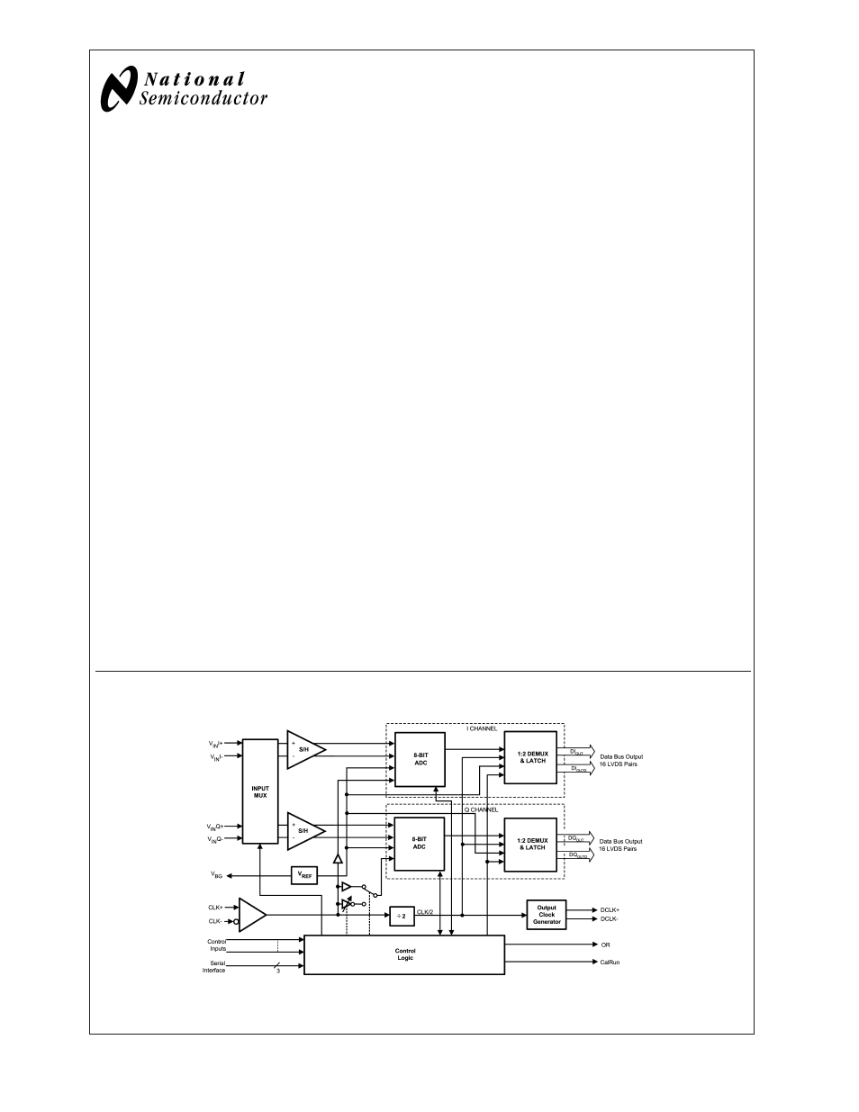
Block Diagram
20097453
ADVANCE INFORMATION
January 2005
High
Performance,
Low
Power
,
Dual
8-Bit,
1
GSPS
A/D
Converter
© 2005 National Semiconductor Corporation
DS200974
www.national.com
Document Outline
- ADC08D1000
- General Description
- Features
- Key Specifications
- Applications
- Block Diagram
- Ordering Information
- Pin Configuration
- Pin Descriptions and Equivalent Circuits
- Absolute Maximum Ratings
- Operating Ratings (Notes , )
- Converter Electrical Characteristics
- Specification Definitions
- Transfer Characteristic
- Timing Diagrams
- FIGURE 3. ADC08D1000 Timing - SDR Clocking
- FIGURE 4. ADC08D1000 Timing - DDR Clocking
- FIGURE 5. Serial Interface Timing
- FIGURE 6. Clock Reset Timing in DDR Mode
- FIGURE 7. Clock Reset Timing in SDR Mode with OUTEDGE Low
- FIGURE 8. Clock Reset Timing in SDR Mode with OUTEDGE High
- FIGURE 9. Self Calibration and On-Command Calibration Timing
- 1.0 Functional Description
- 2.0 Applications Information
- 2.1 THE REFERENCE VOLTAGE
- 2.2 THE ANALOG INPUT
- 2.3 THE CLOCK INPUTS
- 2.4 CONTROL PINS
- 2.5 THE DIGITAL OUTPUTS
- 2.6 POWER CONSIDERATIONS
- 2.7 LAYOUT AND GROUNDING
- 2.8 DYNAMIC PERFORMANCE
- 2.9 USING THE SERIAL INTERFACE
- 2.10 COMMON APPLICATION PITFALLS
- Physical Dimensions