Program cycle characteristics, Program cycle waveforms, Chip erase cycle waveforms – Rainbow Electronics AT49F512 User Manual
Page 7: Program cycle waveforms chip erase cycle waveforms
AT49F512
7
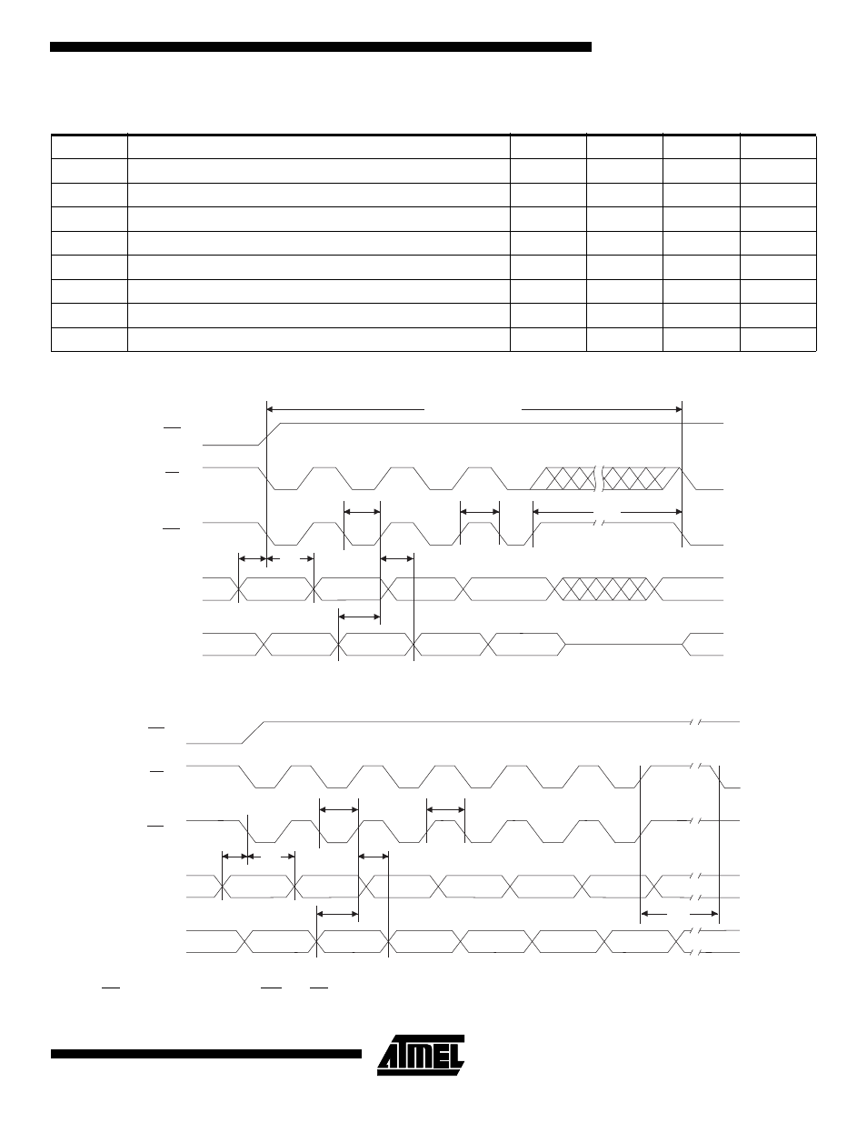
Program Cycle Waveforms
Chip Erase Cycle Waveforms
Note:
OE must be high only when WE and CE are both low.
Program Cycle Characteristics
Symbol
Parameter
Min
Typ
Max
Units
t
BP
Byte Programming Time
10
50
µ
s
t
AS
Address Set-up Time
0
ns
t
AH
Address Hold Time
50
ns
t
DS
Data Set-up Time
50
ns
t
DH
Data Hold Time
0
ns
t
WP
Write Pulse Width
90
ns
t
WPH
Write Pulse Width High
90
ns
t
EC
Erase Cycle Time
10
seconds
OE
PROGRAM CYCLE
INPUT
DATA
ADDRESS
A0
55
5555
5555
AA
2AAA
t
BP
t
WPH
t
WP
CE
WE
A0-A15
DATA
t
AS
t
AH
t
DH
t
DS
OE
AA
80
10
55
55
5555
5555
5555
AA
BYTE 0
BYTE 1
BYTE 2
BYTE 3
BYTE 4
BYTE 5
2AAA
2AAA
t
WPH
t
WP
CE
WE
A0-A15
DATA
t
AS
t
AH
t
EC
t
DH
t
DS
5555
See also other documents in the category Rainbow Electronics Storage:
- W27E010 (14 pages)
- W27L520 (16 pages)
- W29EE512 (21 pages)
- W27E512 (16 pages)
- W24100 (11 pages)
- W27E040 (15 pages)
- W25Q32 (60 pages)
- W49L102 (21 pages)
- W29C040 (20 pages)
- W29EE011 (20 pages)
- W49F020 (21 pages)
- W2465 (10 pages)
- W24256 (10 pages)
- W982516CH (43 pages)
- MAX16014 (12 pages)
- W24512A (10 pages)
- W27E020 (14 pages)
- W29C020C (21 pages)
- W25X64 (47 pages)
- W24257 (11 pages)
- W24L257 (10 pages)
- W9864G2GH (48 pages)
- W24L11 (11 pages)
- W27L010 (14 pages)
- W27E520 (16 pages)
- W27LE520 (16 pages)
- W9825G6CH (43 pages)
- W49F002U (23 pages)
- W9864G6GB (47 pages)
- AT45DB011B (32 pages)
- AT45DB642 (71 pages)
- AT45DB642 (37 pages)
- AT45DB161D (51 pages)
- AT27LV040A (12 pages)
- AT29LV010A (15 pages)
- HT24LC08 (11 pages)
- AT29C257 (12 pages)
- AT45DB161B (32 pages)
- AT27C1024 (12 pages)
- AT28BV256 (12 pages)
- AT28C040 (12 pages)
- DS1258Y_AB (9 pages)
- AT28BV64B (12 pages)
- AT27C512R (12 pages)
- DS1220AB_AD (9 pages)