Block diagram, Device operation, Block diagram device operation – Rainbow Electronics AT49F512 User Manual
Page 2
AT49F512
2
detected by the DATA polling feature. Once the end of a
byte program cycle has been detected, a new access for a
read or program can begin. The typical number of program
and erase cycles is in excess of 10,000 cycles.
The optional 8K bytes boot block section includes a repro-
gramming write lock out feature to provide data integrity.
The boot sector is designed to contain user secure code,
and when the feature is enabled, the boot sector is perma-
nently protected from being reprogrammed.
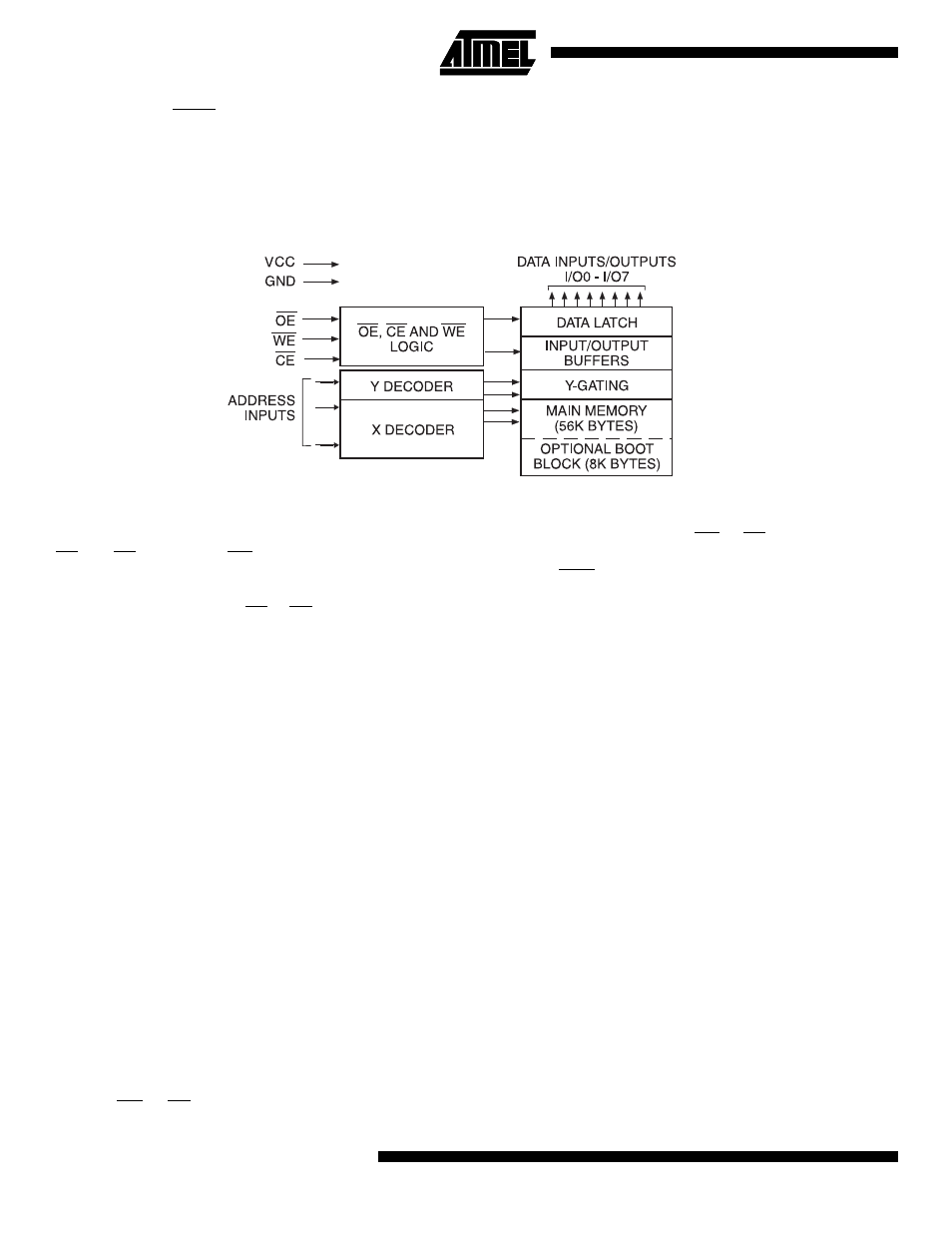
Block Diagram
Device Operation
READ: The AT49F512 is accessed like an EPROM. When
CE and OE are low and WE is high, the data stored at the
memory location determined by the address pins is
asserted on the outputs. The outputs are put in the high
impedance state whenever CE or OE is high. This dual-line
control gives designers flexibility in preventing bus conten-
tion.
ERASURE: Before a byte can be reprogrammed, the 64K
bytes memory array (or 56K bytes if the boot block featured
is used) must be erased. The erased state of the memory
bits is a logical “1”. The entire device can be erased at one
time by using a 6-byte software code. The chip erase code
consists of 6-byte load commands to specific address loca-
tions with a specific data pattern (please refer to the Chip
Erase Cycle Waveforms).
After the chip erase has been initiated, the device will inter-
nally time the erase operation so that no external clocks
are required. The maximum time needed to erase the
whole chip is t
EC
. If the boot block lockout feature has been
enabled, the data in the boot sector will not be erased.
BYTE PROGRAMMING: Once the memory array is
erased, the device is programmed (to a logical “0”) on a
byte-by-byte basis. Please note that a data “0” cannot be
programmed back to a “1”; only erase operations can con-
vert “0”s to “1”s. Programming is accomplished via the
internal device command register and is a 4 bus cycle
operation (please refer to the Command Definitions table).
The device will automatically generate the required internal
program pulses.
The program cycle has addresses latched on the falling
edge of WE or CE, whichever occurs last, and the data
latched on the rising edge of WE or CE, whichever occurs
first. Programming is completed after the specified t
BP
cycle
time. The DATA polling feature may also be used to indicate
the end of a program cycle.
BOOT BLOCK PROGRAMMING LOCKOUT: The device
has one designated block that has a programming lockout
feature. This feature prevents programming of data in the
designated block once the feature has been enabled. The
size of the block is 8K bytes. This block, referred to as the
boot block, can contain secure code that is used to bring up
the system. Enabling the lockout feature will allow the boot
code to stay in the device while data in the rest of the
device is updated. This feature does not have to be acti-
vated; the boot block’s usage as a write protected region is
optional to the user. The address range of the boot block is
0000H to 1FFFH.
Once the feature is enabled, the data in the boot block can
no longer be erased or programmed. Data in the main
memory block can still be changed through the regular pro-
gramming method. To activate the lockout feature, a series
of six program commands to specific addresses with spe-
cific data must be performed. Please refer to the Command
Definitions table.
BOOT BLOCK LOCKOUT DETECTION: A software
method is available to determine if programming of the boot
block section is locked out. When the device is in the soft-
ware product identification mode (see Software Product
Identification Entry and Exit sections) a read from address
location 00002H will show if programming the boot block is
locked out. If the data on I/O0 is low, the boot block can be
programmed; if the data on I/O0 is high, the program lock-
FFFFH
2000H
1FFFH
0000H