Rainbow Electronics AT49F512 User Manual
Features, Description, Pin configurations
1
Features
•
Single Voltage Operation
– 5V Read
– 5V Reprogramming
•
Fast Read Access Time - 50 ns
•
Internal Program Control and Timer
•
8K Bytes Boot Block With Lockout
•
Fast Erase Cycle Time - 10 seconds
•
Byte-by-Byte Programming - 10 µs/Byte
•
Hardware Data Protection
•
DATA Polling For End Of Program Detection
•
Low Power Dissipation
– 30 mA Active Current
– 100 µA CMOS Standby Current
•
Typical 10,000 Write Cycles
Description
The AT49F512 is a 5-volt-only in-system programmable and erasable Flash Memory.
Its 512K of memory is organized as 65,536 words by 8 bits. Manufactured with
Atmel’s advanced nonvolatile CMOS technology, the devices offer access times to 50
ns with a power dissipation of just 165 mW over the commercial temperature range.
When the device is deselected, the CMOS standby current is less than 100 µA.
To allow for simple in-system reprogrammability, the AT49F512 does not require high
input voltages for programming. Five-volt-only commands determine the read and
programming operation of the device. Reading data out of the device is similar to
reading from an EPROM. Reprogramming the AT49F512 is performed by erasing the
entire 512K of memory and then programming on a byte by byte basis. The typical
byte programming time is a fast 10 µs. The end of a program cycle can be optionally
Rev. 1027D–04/99
512K (64K x 8)
5-volt Only
Flash Memory
AT49F512
512K (64K x 8)
5-volt Only
CMOS Flash
Memory
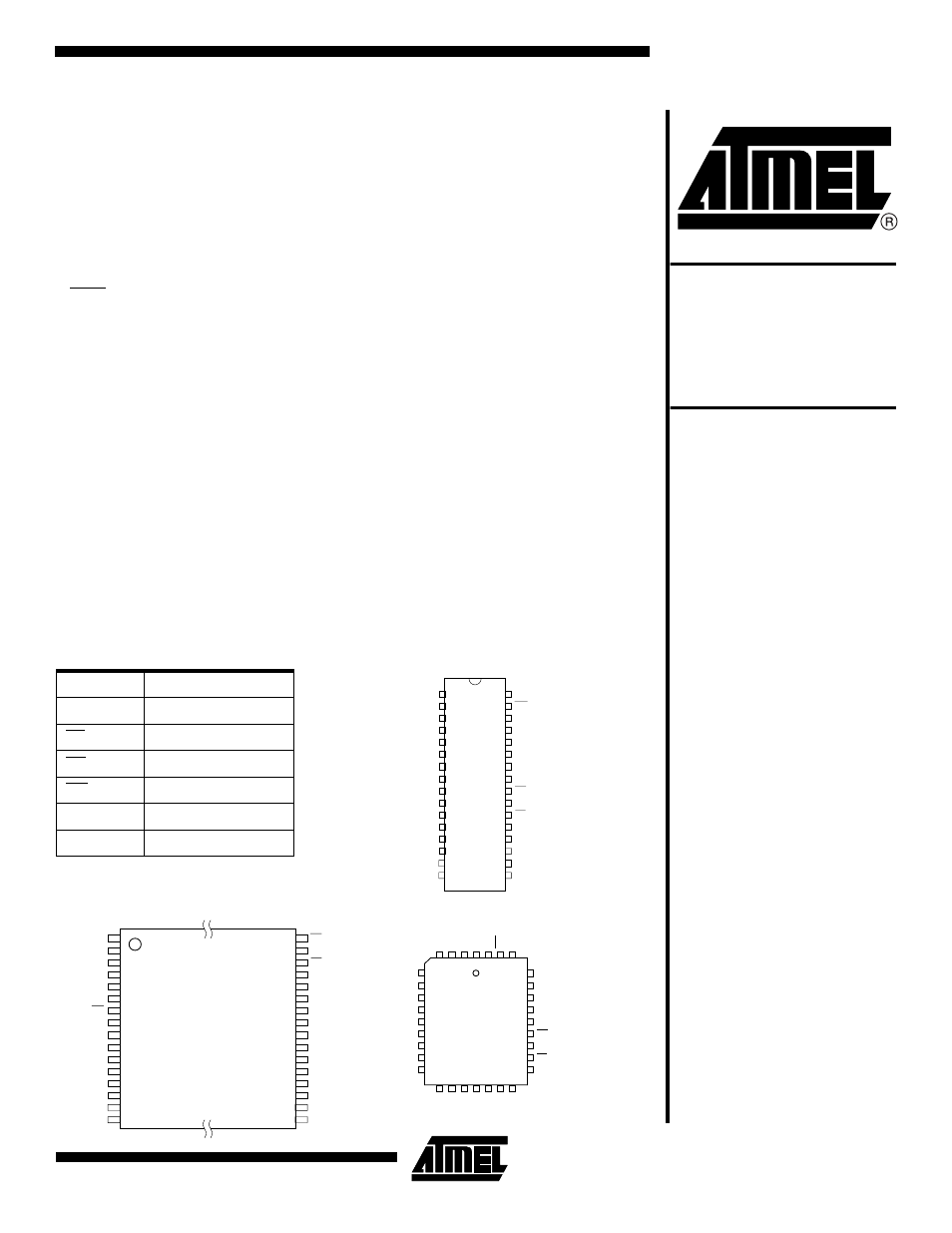
Pin Configurations
Pin Name
Function
A0 - A15
Addresses
CE
Chip Enable
OE
Output Enable
WE
Write Enable
I/O0 - I/O7
Data Inputs/Outputs
NC
No Connect
DIP Top View
1
2
3
4
5
6
7
8
9
10
11
12
13
14
15
16
32
31
30
29
28
27
26
25
24
23
22
21
20
19
18
17
NC
NC
A15
A12
A7
A6
A5
A4
A3
A2
A1
A0
I/O0
I/O1
I/O2
GND
VCC
WE
NC
A14
A13
A8
A9
A11
OE
A10
CE
I/O7
I/O6
I/O5
I/O4
I/O3
PLCC Top View
5
6
7
8
9
10
11
12
13
29
28
27
26
25
24
23
22
21
A7
A6
A5
A4
A3
A2
A1
A0
I/O0
A14
A13
A8
A9
A11
OE
A10
CE
I/O7
4
3
2
1
32
31
30
14
15
16
17
18
19
20
I/O1
I/O2
GND
I/O3
I/O4
I/O5
I/O6
A12
A15
NC
NC
VCC
WE
NC
VSOP Top View (8 x 14 mm) or
TSOP Top View (8 x 20 mm)
Type 1
1
2
3
4
5
6
7
8
9
10
11
12
13
14
15
16
32
31
30
29
28
27
26
25
24
23
22
21
20
19
18
17
A11
A9
A8
A13
A14
NC
WE
VCC
NC
NC
A15
A12
A7
A6
A5
A4
OE
A10
CE
I/O7
I/O6
I/O5
I/O4
I/O3
GND
I/O2
I/O1
I/O0
A0
A1
A2
A3
(continued)
Document Outline
- Pin Configurations
- Features
- Description
- Block Diagram
- Device Operation
- Command Definition (in Hex)
- Absolute Maximum Ratings*
- DC and AC Operating Range
- Operating Modes
- DC Characteristics
- AC Read Characteristics
- AC Read Waveforms(1)(2)(3)(4)
- Input Test Waveforms and Measurement Level
- Output Test Load
- Pin Capacitance
- AC Word Load Characteristics
- AC Byte Load Waveforms
- Program Cycle Characteristics
- Program Cycle Waveforms
- Chip Erase Cycle Waveforms
- Data Polling Characteristics(1)
- Data Polling Waveforms
- Toggle Bit Characteristics(1)
- Toggle Bit Waveforms(1)(2)(3)
- Software Product Identification Entry(1)
- Software Product Identifcation Exit(1)
- Boot Block Lockout Enable Algorithm(1)
- Ordering Information(1)