The adc data register – adcl and adch, Adlar = 0, Adlar = 1 – Rainbow Electronics ATtiny15L User Manual
Page 49: Scanning multiple channels, Attiny15l

49
ATtiny15L
1187E–AVR–06/02
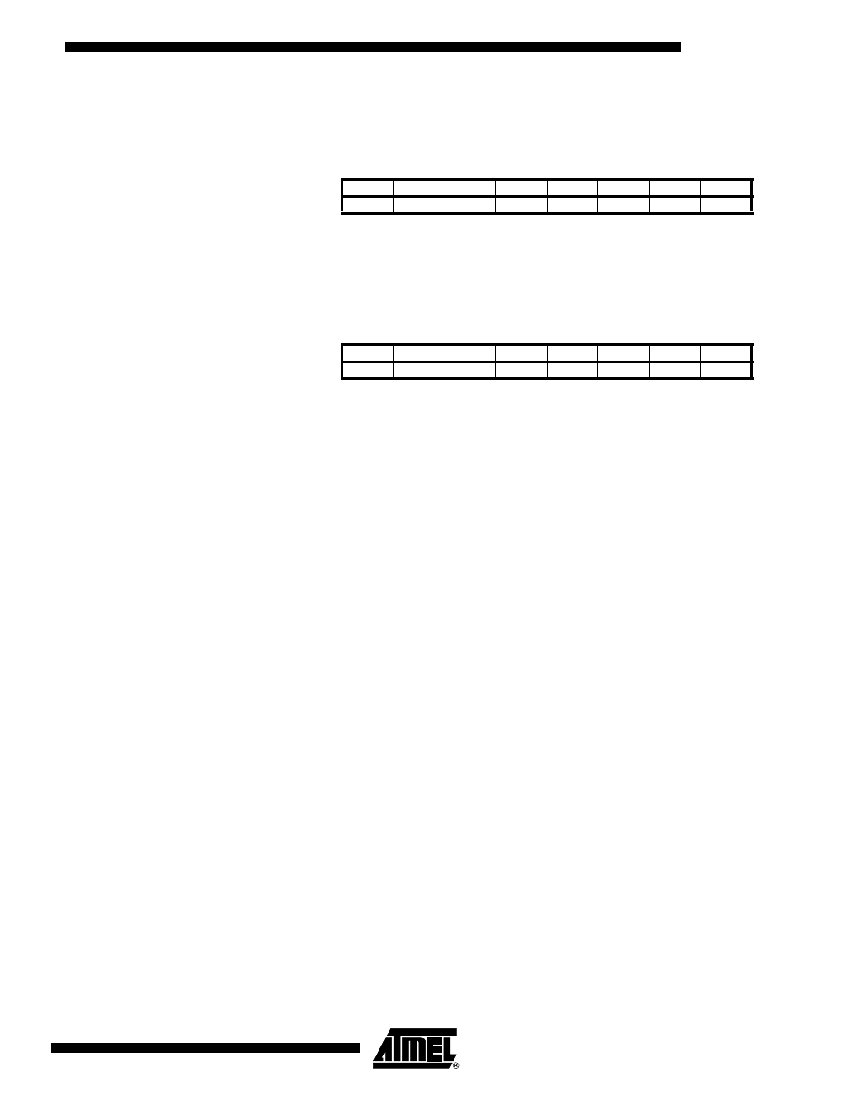
The ADC Data Register –
ADCL and ADCH
ADLAR = 0
ADLAR = 1
When an ADC conversion is complete, the result is found in these two registers. When
ADCL is read, the ADC Data Register is not updated until ADCH is read. If the result is
left adjusted and no more than 8-bit precision is required, it is sufficient to read ADCH.
Otherwise, ADCL must be read first, then ADCH. The ADLAR bit in ADMUX affects the
way the result is read from the registers. If ADLAR is set, the result is left-adjusted. If
ADLAR is cleared (default), the result is right-adjusted.
• ADC9..0: ADC Conversion Result
These bits represent the result from the conversion. For the differential channel, this is
the value after gain adjustment, as indicated in Table 20 on page 47. For single-ended
conversion, or if ADLAR or SIGN is zero, $000 represents ground and $3FF represents
the selected reference voltage minus one LSB.
Scanning Multiple Channels
Since change of analog channel always is delayed until a conversion is finished, the
Free Running mode can be used to scan multiple channels without interrupting the con-
verter. Typically, the ADC Conversion Complete Interrupt will be used to perform the
channel shift. However, the user should take the following fact into consideration:
The interrupt triggers once the result is ready to be read. In Free Running mode, the
next conversion will start immediately when the interrupt triggers. If ADMUX is
changed after the interrupt triggers, the next conversion has already started, and the
old setting is used.
Bit
15
14
13
12
11
10
9
8
$05
–
–
–
–
–
–
ADC9
ADC8
ADCH
$04
ADC7
ADC6
ADC5
ADC4
ADC3
ADC2
ADC1
ADC0
ADCL
7
6
5
4
3
2
1
0
Read/Write
R
R
R
R
R
R
R
R
R
R
R
R
R
R
R
R
Initial Value
0
0
0
0
0
0
0
0
0
0
0
0
0
0
0
0
Bit
15
14
13
12
11
10
9
8
$05
ADC9
ADC8
ADC7
ADC6
ADC5
ADC4
ADC3
ADC2
ADCH
$04
ADC1
ADC0
–
–
–
–
–
–
ADCL
7
6
5
4
3
2
1
0
Read/Write
R
R
R
R
R
R
R
R
R
R
R
R
R
R
R
R
Initial Value
0
0
0
0
0
0
0
0
0
0
0
0
0
0
0
0
