The timer/counter1 control register – tccr1, Attiny15l – Rainbow Electronics ATtiny15L User Manual
Page 29

29
ATtiny15L
1187E–AVR–06/02
The Timer/Counter1 contains two Output Compare Registers, OCR1A and OCR1B, as
the data source to be compared with the Timer/Counter1 contents. In Normal mode the
Output Compare function is operational with OCR1A only, and the Output Compare
function includes optional clearing of the counter on compare match, and action on the
Output Compare pin (PB1) (OC1A).
In PWM mode OCR1A provides the data value against which the Timer/Counter value is
compared. Upon compare match the PWM output is generated. In PWM mode The
Timer/Counter counts up to the value specified in Output Compare Register OCR1B
and starts again from $00. This feature allows limiting the counter “full” value to a speci-
fied value, lower than $FF. Together with the many prescaler options, flexible PWM
frequency selection is provided. Table 14 lists clock selection and OCR1B values to
obtain PWM frequencies from 10 kHz to 150 kHz at 10 kHz steps.
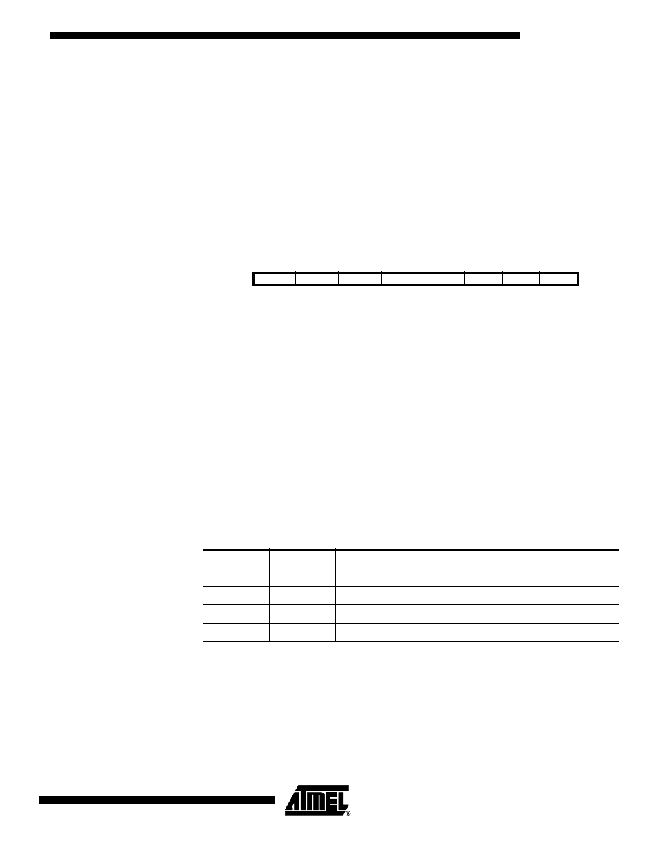
The Timer/Counter1 Control
Register – TCCR1
• Bit 7 – CTC1: Clear Timer/Counter on Compare Match
When the CTC1 control bit is set (one), Timer/Counter1 is reset to $00 in the CPU clock
cycle after a compare match with OCR1A Register value. If the control bit is cleared,
Timer/Counter1 continues counting and is unaffected by a compare match.
• Bit 6 – PWM1: Pulse Width Modulator Enable
When set (one), this bit enables PWM mode for Timer/Counter1. This mode is described
on page 31.
• Bits 5,4 – COM1A1, COM1A0: Compare Output Mode, Bits 1 and 0
The COM1A1 and COM1A0 control bits determine any output pin action following a
compare match A in Timer/Counter1. Output pin actions affect pin PB1(OC1A). Since
this is an alternative function to an I/O port, the corresponding direction control bit must
be set (one) to control an output pin. The control configuration is shown in Table 10.
Note:
1. In PWM mode, these bits have a different function. Refer to Table 12 for a detailed
description.When changing the COM1A1/COM1A0 bits, the Output Compare 1A
Interrupt must be disabled by clearing its Interrupt Enable bit in the TIMSK Register.
Otherwise an interrupt can occur when the bits are changed.
Bit
7
6
5
4
3
2
1
0
$30
CTC1
PWM1
COM1A1
COM1A0
CS13
CS12
CS11
CS10
TCCR1
Read/Write
R/W
R/W
R/W
R/W
R/W
R/W
R/W
R/W
Initial Value
0
0
0
0
0
0
0
0
Table 10. Compare Mode Select
(1)
COM1A1
COM1A0
Description
0
0
Timer/Counter disconnected from output pin OC1A
0
1
Toggle the OC1A output line.
1
0
Clear the OC1A output line (to zero).
1
1
Set the OC1A output line (to one).
