Ata6823 [preliminary, Pin configuration – Rainbow Electronics ATA6823 User Manual
Page 3
3
4856E–AUTO–07/07
ATA6823 [Preliminary]
2.
Pin Configuration
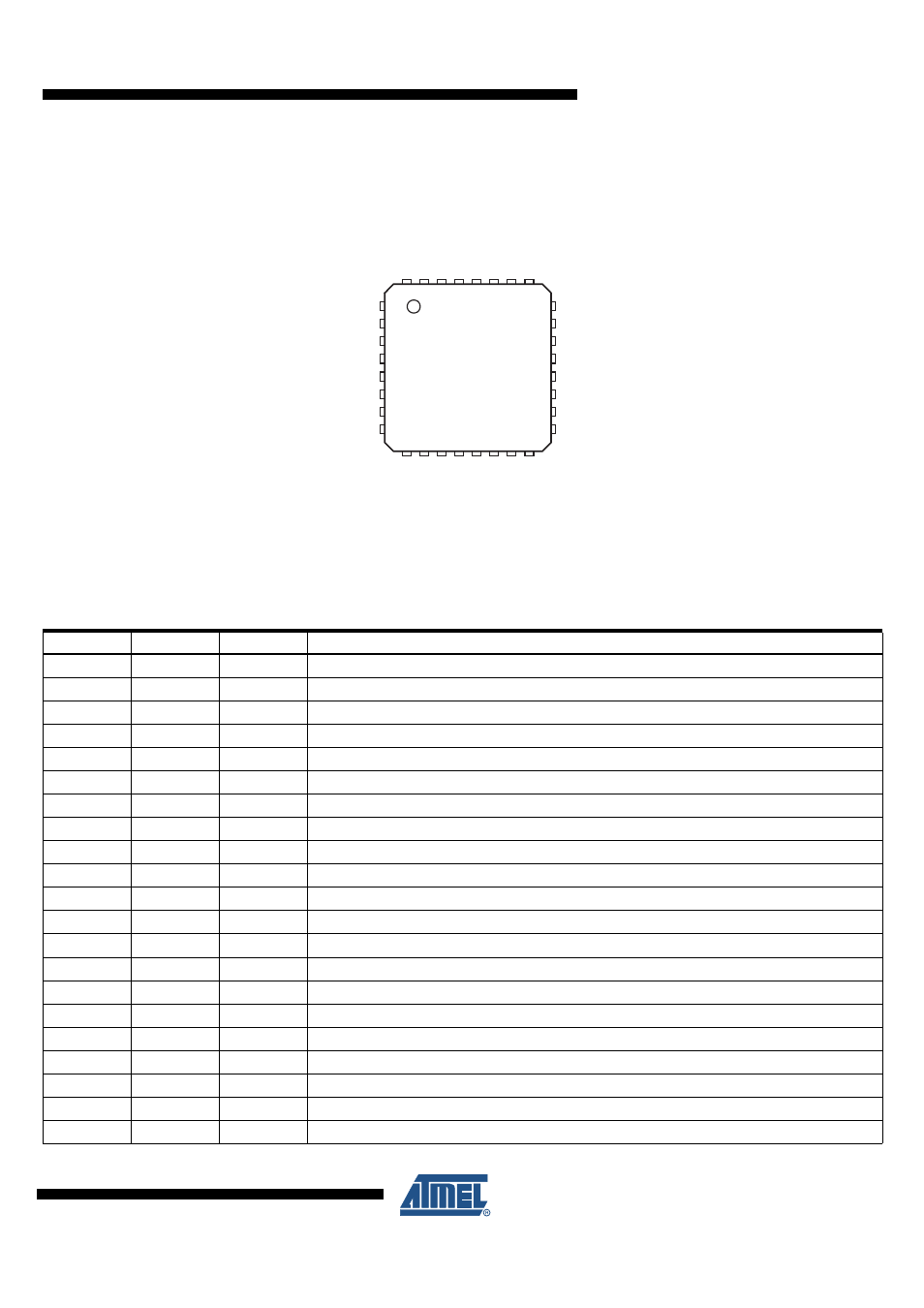
Figure 2-1.
Pinning QFN32
Note:
YWW
Date code (Y = Year - above 2000, WW = week number)
ATA6823 Product
name
ZZZZZ
Wafer lot number
AL
Assembly sub-lot number
VMODE
VINT
RWD
CC
/RESET
WD
GND
LIN
VG
CPLO
CPHI
VRES
H2
S2
H1
S1
EN2
VBATSW
VBAT
VCC
PGND
L1
L2
PBAT
TX
DIR
PWM
EN1
RX
DG3
DG2
DG1
32 31 30 29 28 27 26 25
9 10 11 12 13 14 15 16
1
2
3
4
5
6
7
8
24
23
22
21
20
19
18
17
Atmel YWW
ATA6823
ZZZZZ-AL
Table 2-1.
Pin Description
Pin
Symbol
I/O
Function
1
VMODE
I
Selector for V
CC
and interface logic voltage level
2
VINT
I/O
Blocking capacitor 220 nF/10V/X7R
3
RWD
I
Resistor defining the watchdog interval
4
CC
I/O
RC combination to adjust cross conduction time
5
/RESET
O
Reset signal for microcontroller
6
WD
I
Watchdog trigger signal
7
GND
I
Ground for chip core
8
LIN
I/O
LIN-bus terminal
9
TX
I
Transmit signal to LIN bus from microcontroller
10
DIR
I
Defines the rotation direction for the motor
11
PWM
I
PWM input controls motor speed
12
EN1
I
Microcontroller output to keep the chip in Active mode
13
RX
O
Receive signal from LIN bus for microcontroller
14
DG3
O
Diagnostic output 3
15
DG2
O
Diagnostic output 2
16
DG1
O
Diagnostic output 1
17
S1
I/O
Source voltage H-bridge, high-side 1
18
H1
O
Gate voltage H-bridge, high-side 1
19
S2
I/O
Source voltage H-bridge, high-side 2
20
H2
O
Gate voltage H-bridge, high-side 2
21
VRES
I/O
Gate voltage for reverse protection NMOS, blocking capacitor 470 nF/25V/X7R