Ata6823 [preliminary, Electrical characteristics (continued) – Rainbow Electronics ATA6823 User Manual
Page 22
22
4856E–AUTO–07/07
ATA6823 [Preliminary]
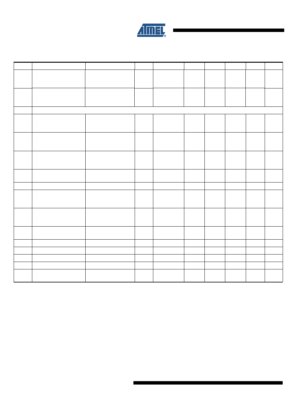
7.12
Static high-side switch
output high-voltage pins
H1, H2
I
Lx
= –10 µA
(PWM = static)
V
HxHstat1
(7)
V
VBAT
+
V
VG
– 1
V
VBAT
+
V
VG
V
7.13
Sink resistance between
Hx and ground in Sleep
mode
R
Hxsleep
3
10
k
Ω
Dynamic Parameters
7.14
Dynamic high-side switch
output high-voltage pins
H1, H2
C
Hx
= 5 nF
C
CB
= 100 nF
f
PWM
= 20 kHz
V
HxHdyn1
V
VBAT
+
V
VG
– 1
V
VBAT
+
V
VG
V
7.15
Propagation delay time,
low-side driver from high
to low
V
VBAT
= 13.5V
t
LxHL
0.5
µs
7.16
Propagation delay time,
low-side driver from low to
high
t
LxLH
0.5 + t
CC
µs
7.17
Fall time low-side driver
V
VBAT
= 13.5V
C
Gx
=5 nF
t
Lxf
0.5
µs
7.18
Rise time low-side driver
t
Lxr
0.5
µs
7.19
Propagation delay time,
high-side driver from high
to low
V
VBAT
= 13.5V
t
HxHL
0.5
µs
7.20
Propagation delay time,
high-side driver from low
to high
t
HxLH
0.5 + t
CC
µs
7.21
Fall time high-side driver
V
VBAT
= 13.5V,
C
Gx
= 5 nF
t
Hxf
0.5
µs
7.22
Rise time high-side driver
t
Hxr
0.5
µs
7.23
Cross conduction time
(8)
t
CC
10
µs
7.24
External resistor
R
CC
5
k
Ω
7.25
External capacitor
C
CC
5
nF
7.26
R
ON
of t
CC
switching
transistor
R
ONCC
100
Ω
9.
Electrical Characteristics (Continued)
All parameters given are valid for 7V
≤
VBAT
≤
18V and for –40°C
≤ ϑ
ambient
≤
125°C unless stated otherwise.
No.
Parameters
Test Conditions
Pin
Symbol
Min
Typ
Max
Unit
Type*
* Type: A = 100% tested, B = 100% correlation tested, C = Characterized on samples, D = Design parameter
Notes:
1. EN, DIR, PWM = high
2. The use of X7R material is recommended
3. For higher values, stability at zero load is not guaranteed
4. Tested during qualification only
5. Value depends on T
OSC
; function tested with digital test pattern
6. Tested during characterization only
7. Supplied by charge pump
8. See section
“Cross Conduction Time”
9. Voltage between source-drain of external switching transistors in active case
10. The short-circuit message will never be generated for switch-on time < t
sc