Ata6823 [preliminary, 6 lin transceiver – Rainbow Electronics ATA6823 User Manual
Page 10
10
4856E–AUTO–07/07
ATA6823 [Preliminary]
After ramp-up of the battery voltage (power-on reset), the V
CC
regulator is switched on. The
reset output, /RESET, stays low for the time t
res
(typically 68 ms), then switches to high. For an
initial lead time t
d
(typically 68 ms for setups in the controller) the watchdog waits for a rising
edge on WD to start its normal window watchdog sequence. If no rising edge is detected, the
watchdog will reset the microcontroller for t
res
and wait t
d
for the rising edge on WD.
Times t
1
(close window) and t
2
(open window) form the window watchdog sequence. To avoid
receiving a reset from the watchdog, the triggering signal from the microcontroller must hit the
timeframe of t
2
= 9.61 ms. The trigger event will restart the watchdog sequence.
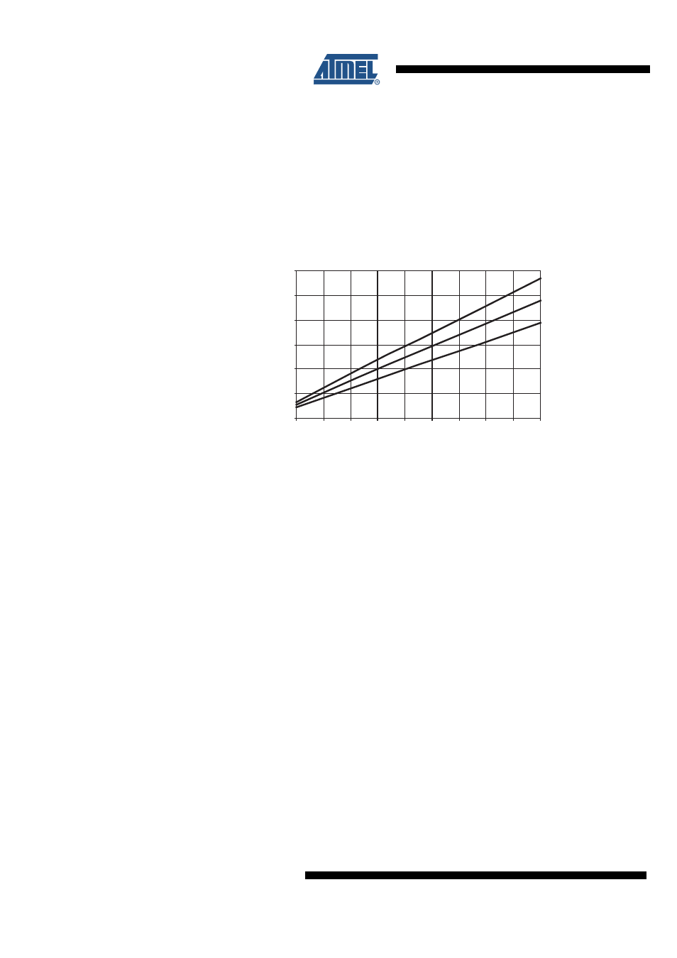
Figure 5-3.
T
WD
versus R
WD
If triggering fails, /RESET will be pulled to ground for a shortened reset time of typically 2 ms.
The watchdog start sequence is similar to the power-on reset.
The internal oscillator is trimmed to a tolerance of < ±10%. This means that t
1
and t
2
can also
vary by ±10%. The following calculation shows the worst case calculation of the watchdog
period T
wd
which the microcontroller has to provide.
t
1min
= 0.90
×
t
1
= 10.87 ms, t
1max
= 1.10
×
t
1
= 13.28 ms
t
2min
= 0.90
×
t
2
= 8.65ms, t
2max
= 1.10
×
t
2
= 10.57 ms
T
wdmax
= t
1min
+ t
2min
= 10.87 ms + 8.65 ms = 19.52 ms
T
wdmin
= t
1max
= 13.28 ms
T
wd
= 16.42 ms ±3.15 ms (±19.1%)
above shows the typical watchdog period T
WD
depending on the value of the external
resistor R
OSC
.
A reset will be active for V
CC
< V
tHRESx
; the level V
tHRESx
is realized with a hysteresis (HYS
RESth
).
5.6
LIN Transceiver
A bi-directional bus interface is implemented for data transfer between the LIN bus and the local
LIN protocol controller.
The transceiver consists of a low side driver (1.2V at 40 mA) with slew rate control, wave shap-
ing, current limitation, and a high-voltage comparator followed by a debouncing unit in the
receiver.
RWD (k
Ω
)
TWD (ms)
max
min
0
10
20
30
40
50
60
10
20
30
40
50
60
70
80
90
100
typ