Ata6823 [preliminary, 7 control inputs en1, en2, dir, pwm – Rainbow Electronics ATA6823 User Manual
Page 12
12
4856E–AUTO–07/07
ATA6823 [Preliminary]
5.7
Control Inputs EN1, EN2, DIR, PWM
5.7.1
Pins EN1, EN2
Any of the enable pins may be used to activate the IC with a HIGH. EN1 is a low level input, EN2
has to withstand a voltage up to 40V. Internal pull-down resistors are included.
5.7.2
Pin DIR
Logical input to control the direction of the external motor to be controlled by the IC. An internal
pull-down resistor is included.
5.7.3
Pin PWM
Logical input for PWM information delivered by external microcontroller. Duty cycle and fre-
quency at this pin are passed through to the H-bridge. An internal pull-down resistor is included.
The internal signal ON is high when
• At least one valid trigger has been accepted (SYNC = 1)
• V
BAT
is inside the specified range (UV = 0 and nOV = 1)
• The charge pump has reached its minimum voltage (CPOK = 1) and
• The device is not overheated (OT2 = 0)
In case of a short circuit, the appropriate transistor is switched off after a debounce time of about
10 µs. In order to avoid cross current through the bridge, a cross conduction timer is imple-
mented. Its time constant is programmable by means of an RC combination.
In order to be able to distinguish between a wake-up from LIN or from EN2, the source of
wake-up is flagged in DG1 until the first valid trigger (LIN = 0, EN2 = 1).
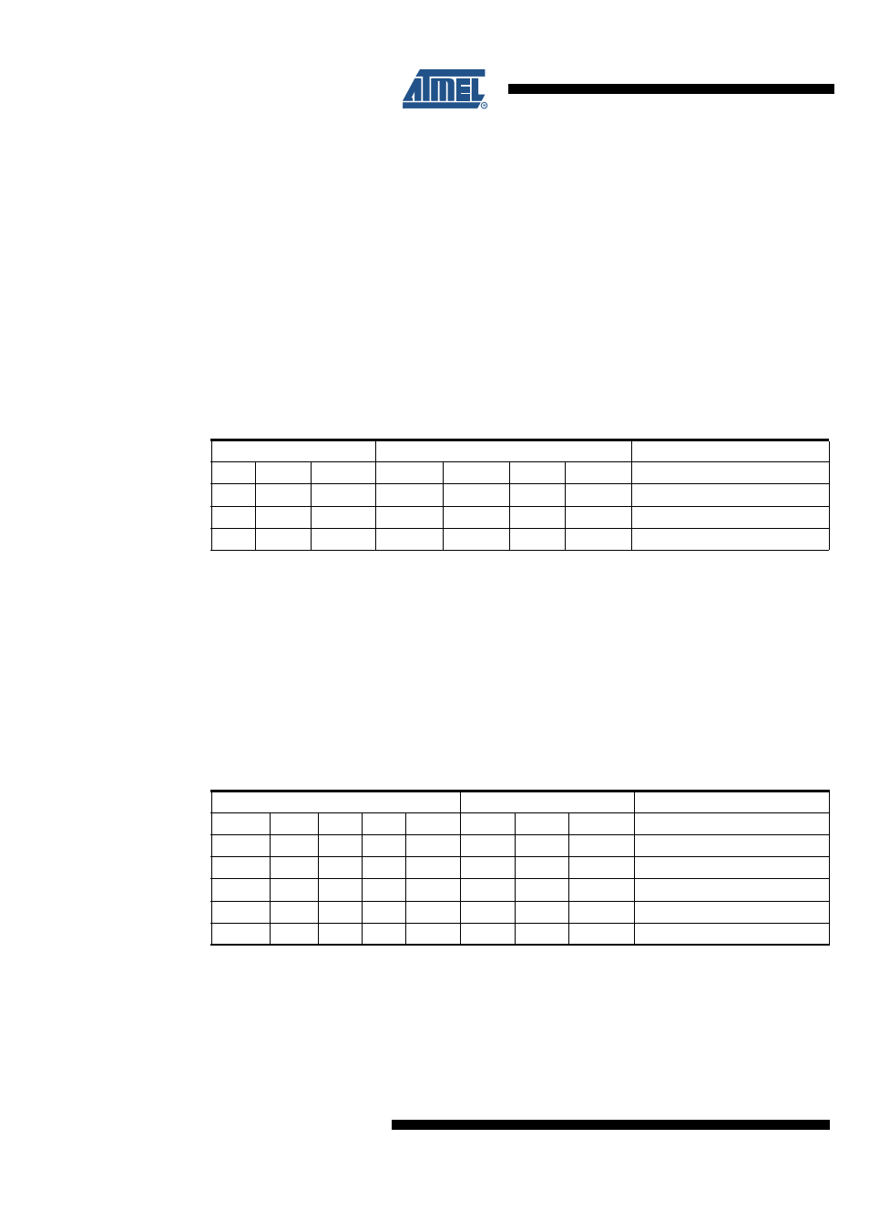
Table 5-1.
Status of the IC Depending on Control Inputs and Detected Failures
Control Inputs
Driver Stage for External Power MOS
Comments
ON
DIR
PWM
H1
L1
H2
L2
0
X
X
OFF
OFF
OFF
OFF
Standby mode
1
0
PWM
ON
OFF
/PWM
PWM
Motor PWM forward
1
1
PWM
/PWM
PWM
ON
OFF
Motor PWM reverse
Table 5-2.
Status of the Diagnostic Outputs
Device Status
Diagnostic Outputs
Comments
CPOK
OT1
OV
UV
SC
DG1
DG2
DG3
0
X
X
X
X
–
1
–
Charge pump failure
X
1
X
X
X
–
–
1
Overtemperature warning
X
X
1
X
X
–
1
–
Overvoltage
X
X
X
1
X
–
1
–
Undervoltage
X
X
X
X
1
1
–
–
Short circuit
Note:
X represents: don't care – no effect)
OT1: Overtemperature warning
OV: Overvoltage of VBAT
UV: Undervoltage of VBAT
SC: Short circuit
CPOK: Charge pump OK