Rc2100 – Rainbow Electronics RC2100 User Manual
Page 4
RC2100
2005 Radiocrafts AS
RC2100 Data Sheet (rev. 1.0)
Page 4 of 22
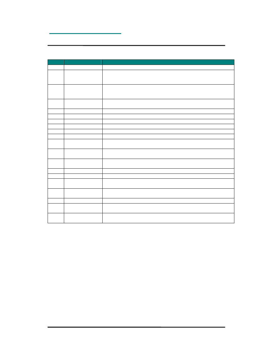
Pin Description
Pin no Pin name
Description
1
GND
System ground
2
CTS/RXTX/RXEN UART Clear to Send, UART RXTX (for RS485), Receive Mode
Enable, or SLEEP mode activation. Connect to VDD if not used.
Internal 100 k series resistor, 2.7 V output.
3
RTS/TXEN
UART Request to Send, Transmit Mode Enable, or SLEEP mode
activation. Connect to VDD if not used. Internal 100 k series
resistor.
4
CONFIG
Configuration Enable. Active low. Should normally be set high.
Connect to VDD if not used. Internal 100 k series resistor.
5
TXD
UART TX Data. Internal 100 k series resistor, 2.7 V output.
6
RXD
UART RX Data. Internal 100 k series resistor.
7
GND
System ground
8
GND
System ground
9
RF
RF I/O connection to antenna
10
GND
System ground
11
VDD
Supply voltage output, regulated 2.7 V. Should normally be left open
if not used for pull-ups.
12
ON/OFF
Module on/off (shutdown). ON when high, OFF when low. See also
important note under Power Management page 12.
13
VCC
Supply voltage input. Internally regulated. Maximum rise-time
requirement apply, see Electrical Specification.
14
GND
System ground
15-21 RESERVED
Test pins, or pins reserved for internal/future use.
Do not connect!
22
RESET
Main reset (active low). Should normally be left open. Internal 100 k
pull-up resistor, no series resistor.
23
CCA/PA_EN
Clear Channel Assessment (active high) or External PA Enable
output (active low). No internal series resistor or pull-up, 2.7 V output.
24-28 RESERVED
Test pins, or pins reserved for internal/future use.
Do not connect!
29
SCL
Transparent synchronous serial data clock. No internal series resistor
or pull-up, 2.7 V output.
30
SDA
Transparent synchronous serial data I/O. No internal series resistor
or pull-up, 2.7 V input/output.
Note 1: In UART mode the TXD and RXD are used for serial data, and CTS/RXTX and RTS for flow control
(optional). If flow control is not used, and RXEN and TXEN are both asserted (active low) the module is set in SLEEP
mode. RXEN and TXEN should be connected to VDD if not to be used for SLEEP mode activation. A pull-up resistor
is not necessary due to an internal series resistor.
Note 2: In synchronous mode the SCL (data clock output) and SDA (Data input and output) are used for serial data.
The RXEN and TXEN pins are then used to select the operation mode of the device. Signals are active low.
Note 3: The CONFIG pin is used to enter configuration mode (change of default settings). Active low.
Note 4: Do not use VDD for supply to external circuits. Should only be used for pull-ups, if required.
Note 5: RXEN, TXEN, CONFIG, TXD and RXD have internal 100 k series resistors. Driving capability when used as
outputs is therefore limited and should be connected to CMOS inputs only.