Electrical characteristics (continued) – Rainbow Electronics MAX8775 User Manual
Page 6
MAX8775
Dual and Combinable Graphics Core
Controller for Notebook Computers
6
_______________________________________________________________________________________
Note 1: When the inductor is in continuous conduction, the output voltage has a DC regulation level lower than the error comparator
threshold by 50% of the ripple. In discontinuous conduction, the output voltage has a DC regulation level higher than the
error comparator threshold by 50% of the ripple.
Note 2: Operation below 0.5V but above the REFOK threshold is allowed, but the accuracy is not guaranteed.
Note 3: The MAX8775 cannot operate over all combinations of frequency, input voltage (V
IN
), and output voltage. For large input-to-
output differentials and high switching-frequency settings, the required on-time might be too short to maintain the regulation
specifications. Under these conditions, a lower operating frequency must be selected. The minimum on-time must be
greater than 150ns, regardless of the selected switching frequency. On-time and off-time specifications are measured from
the 50% point to the 50% point at the DH_ pin with LX_ = GND, VBST_ = 5V, and a 250pF capacitor connected from DH_ to
LX_. Actual in-circuit times may differ due to MOSFET switching speeds.
Note 4: Specifications are guaranteed by design, not production tested.
Note 5: Production testing limitations due to package handling require relaxed maximum on-resistance specifications for the
thin QFN package.
Note 6: Specifications to T
A
= -40°C to +85°C are guaranteed by design, not production tested.
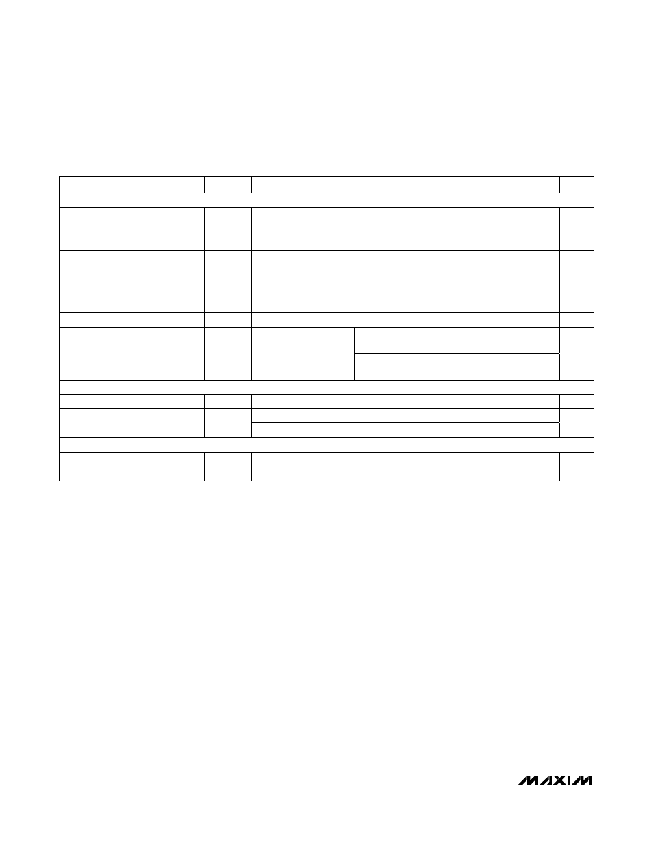
ELECTRICAL CHARACTERISTICS (continued)
(Circuit of Figure 1, V
IN
= 12V,
SKIP_ = 0, ON_ = V
CC
= 5V, separate mode, T
A
= -40°C to +85°C, unless otherwise noted.) (Note 6)
PARAMETER
SYMBOL
CONDITIONS
MIN
TYP
MAX
UNITS
FAULT DETECTION
OVP_ Adjust Range
V
OVP_
0.5
2.5
V
O utp ut O ver vol tag e Tr i p Thr eshol d
Rising edge measured at CSL_,
with respect to OVP_ set voltage
180
220
mV
Output Undervoltage Protection
Trip Threshold
Falling edge measured at CSL_,
with respect to error comparator threshold
275
325
mV
PGOOD_ Lower Trip Threshold
Falling edge measured at CSL_
with respect to error comparator threshold,
hysteresis = 1%
-180
-120
mV
PGOOD_ Output Low Voltage
I
SINK
= 4mA
0.4
V
Lower threshold,
0.84V
REF
2.0
2.2
Current-Balance Fault
Comparator Thresholds
V(CCI2, REF),
0.5V
≤ V
FB
≤ 2.5V
Upper threshold,
1.2V
REF
2.9
3.1
mV
GATE DRIVERS
DH_ Gate Driver On-Resistance
R
DH
BST_ - LX_ forced to 5V (Note 4)
5
Ω
DL_, high state
5
DL_ Gate Driver On-Resistance
(Note 4)
R
DL
DL_, low state
3
Ω
INPUTS AND OUTPUTS
Logic Input-High Threshold
ON1, ON2,
DTRANS, SKIP1, SKIP2,
hysteresis = 225mV
1.2
2.2
V