Electrical characteristics (continued) – Rainbow Electronics MAX8775 User Manual
Page 4
MAX8775
Dual and Combinable Graphics Core
Controller for Notebook Computers
4
_______________________________________________________________________________________
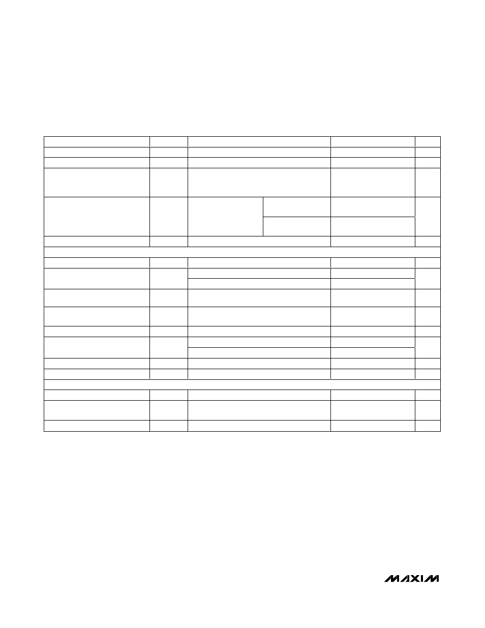
ELECTRICAL CHARACTERISTICS (continued)
(Circuit of Figure 1, V
IN
= 12V,
SKIP_ = PGND = AGND, ON_ = V
CC
= 5V, separate mode, T
A
= 0°C to +85°C, unless otherwise
noted. Typical values are at T
A
= +25°C.)
PARAMETER
SYMBOL
CONDITIONS
MIN
TYP
MAX
UNITS
PGOOD_ Output Low Voltage
I
SINK
= 4mA
0.4
V
PGOOD_ Leakage Current
I
PGOOD
_
High state, PGOOD_ forced to 5.5V
1
µA
PGOOD_ Transition Blanking
Time
Measured from the time CSL_ reaches the
target voltage based on the slew rate set by
C
SLEW_
20
µs
Lower threshold,
0.84V
REF
2.0
2.2
Current-Balance Fault
Comparator Thresholds
V(CCI2, REF),
0.5V
≤
V
FB
≤ 2.5V
Upper threshold,
1.2V
REF
2.9
3.0
V
Thermal-Shutdown Threshold
T
SHDN
Hysteresis = 15°C
+160
°C
GATE DRIVERS
DH_ Gate Driver On-Resistance
R
DH
BST_ - LX_ forced to 5V (Note 5)
1.5
5
Ω
DL_, high state
1.7
5
DL_ Gate Driver On-Resistance
(Note 5)
R
DL
DL_, low state
0.6
3
Ω
DH_ Gate Driver Source/
Sink Current
I
DH
DH_ forced to 2.5V, BST_ - LX_ forced to 5V
2
A
DL_ Gate Driver Source Current
I
DL
(SOURCE)
DL_ forced to 2.5V
1.7
A
DL_ Gate Driver Sink Current
I
DL (SINK)
DL_ forced to 2.5V
3.3
A
DL_ to DH_
15
35
Dead Time
t
DEAD
DH_ to DL_
10
26
ns
Internal Boost Diode Switch R
ON
Measure with 10mA of current
6.5
9
Ω
LX_, BST_ Leakage Current
V
BST
_ = V
LX
_ = 28V
< 2
20
µA
INPUTS AND OUTPUTS
Logic Input Current
ON1, ON2,
DTRANS, SKIP1, SKIP2
-1
+1
µA
Logic Input-High Threshold
ON1, ON2,
DTRANS, SKIP1, SKIP2,
hysteresis = 225mV
1.2
1.7
2.2
V
Input Leakage Current
CSH_, CSL_, 0V, or V
DD
-0.15
+0.15
µA