Electrical characteristics – Rainbow Electronics MAX8775 User Manual
Page 5
MAX8775
Dual and Combinable Graphics Core
Controller for Notebook Computers
_______________________________________________________________________________________
5
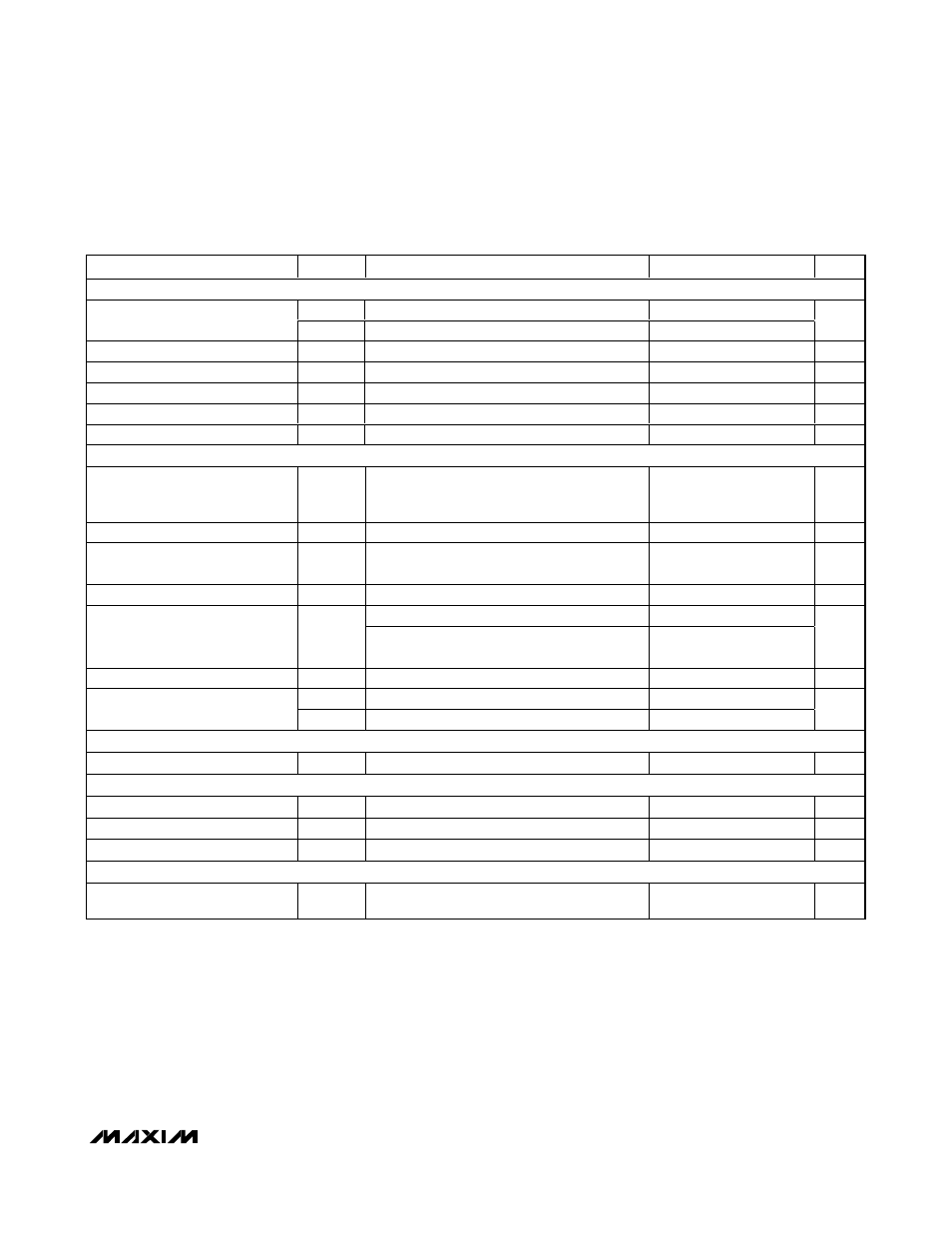
ELECTRICAL CHARACTERISTICS
(Circuit of Figure 1, V
IN
= 12V,
SKIP_ = 0, ON_ = V
CC
= 5V, separate mode, T
A
= -40°C to +85°C, unless otherwise noted.) (Note 6)
PARAMETER
SYMBOL
CONDITIONS
MIN
TYP
MAX
UNITS
INPUT SUPPLIES
V
IN
4
26
Input Voltage Range
V
BIAS
V
CC
, V
DD
4.5
5.5
V
V
CC
Undervoltage Lockout
V
UVLO
Rising edge, 200mV typical hysteresis
4.1
4.5
V
Quiescent Supply Current (V
CC
)
I
CC
CSL_ forced above their regulation points
2.5
mA
Quiescent Supply Current (V
DD
)
I
DD
CSL_ forced above their regulation points
5
µA
Shutdown Supply Current (V
CC
)
ON1 = ON2 = GND
5
µA
Shutdown Supply Current (V
DD
)
ON1 = ON2 = GND
5
µA
MAIN SMPS CONTROLLERS
PWM_ Output Voltage
V
REFIN_
-
V
CSL_
With respect to REFIN_,
REFIN_ = 0.5V to 2.5V,
SKIP_ = V
CC
or GND (Note 1)
-7.5
+7.5
mV
Output Voltage Adjust Range
V
CSL_
Either SMPS (Note 2)
0.5
2.5
V
REFIN Operating Voltage Adjust
Range
V
REFIN_
Either SMPS (Note 2)
0.5
2.5
V
Combined Mode Enabled
V
REFIN2
3
V
R
OSC
= 143k
Ω (f
OSC
= 300kHz nominal)
-15
+15
Switching Frequency Accuracy
(Note 2)
f
OSC
R
OSC
= 71.5k
Ω (f
OSC
= 600kHz nominal) to
432k
Ω (f
OSC
= 99kHz nominal)
-20
+20
%
Maximum Duty Factor
D
MAX
90
%
I
SLEW_
During transition
3.75
5.50
Slew-Rate Current
I
SLEWSS_
Startup and shutdown
0.7
1.2
µA
CURRENT LIMIT
Current-Limit Threshold
V
LIMIT
V
CSH
_ - V
CSL
_
25
35
mV
REFERENCE (REF)
Reference Voltage
V
REF
V
CC
= 4.5V to 5.5V, I
REF
= 0
2.462
2.538
V
Refer ence S our ce Load Reg ul ati on
ΔV
REF
I
REF
= 0µA to 250µA
2
mV
Reference Sink Load Regulation
I
REF
= -50µA
10
mV
CURRENT BALANCE
Current-Balance Amplifier (GMI)
Offset
[V(CSH1,CSL1) - V(CSH2,CSL2)] at I
CCI
= 0
-3
+3
mV