Rainbow Electronics MAX8775 User Manual
Page 13
output voltages required by the different GPU operating
and sleep states. Automatic fault blanking, forced-PWM
operation, and transition control are achieved by
detecting the voltage change at REFIN.
The interleaved, fixed-frequency architecture provides
180° out-of-phase operation to reduce the input capaci-
tance required to meet the RMS input-current ratings.
Each controller consists of a multi-input PWM compara-
tor, high-side and low-side gate drivers, fault protec-
tion, power-good detection, soft-start, and shutdown
logic. Current-mode control allows the use of low-ESR
output capacitors.
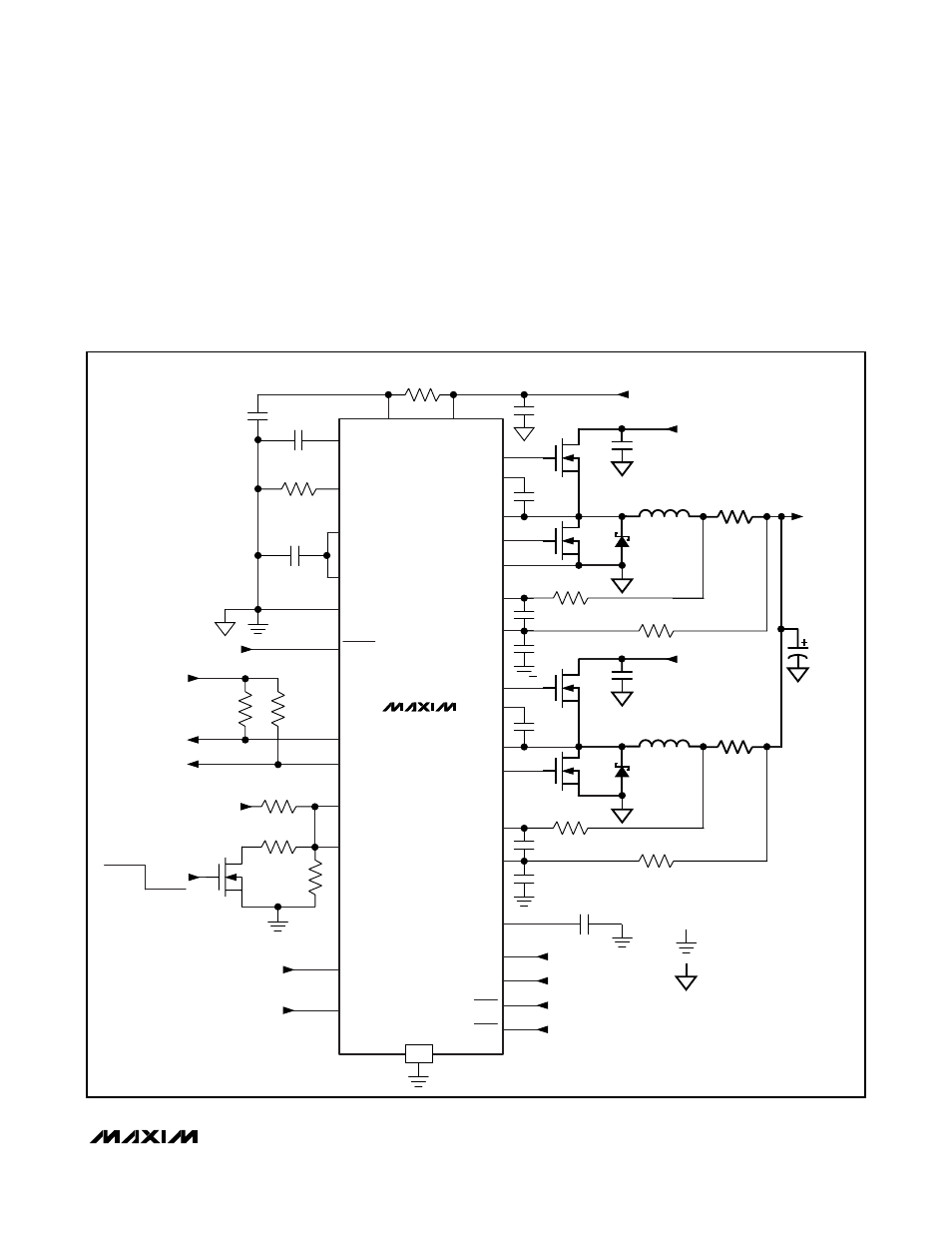
In combined mode (Figure 2), phase 1 provides the
main voltage-control loop while phase 2 maintains the
MAX8775
Dual and Combinable Graphics Core
Controller for Notebook Computers
______________________________________________________________________________________
13
V
DD
V
CC
C4
1
μF
OSC
R
OSC
154k
Ω
CCI2
REF
R7
10
Ω
PGOOD1
+5V
R8
100k
Ω
PGOOD2
GND
SKIP1
SKIP2
ON1
ON2
SLEW1
C
REF
0.1
μF
SLEW2
NOT USED
DTRANS
C
BST1
0.1
μF
+5V
LX1
DH1
BST1
DL1
CSL1
CSH1
C3
2.2
μF
INPUT V
IN
7V TO 20V
L1
0.56
μH
D
L1
C
IN1
N
H1
N
L1
V
OUT
1.5V/1.2V 40A
CSL2
CSH2
LX2
DH2
BST2
DL2
ANALOG GROUND
POWER GROUND
R
SENSE1
1.0m
Ω
R10
100
Ω
R11
10
Ω
C1
2.2nF
C2
4.7nF
R1
100k
Ω
OVP1
REFIN1
REF
REF
V
CC
V
OUT(L)
V
OUT(H)
CONNECT REFIN2 TO V
CC
AND
OVP2 TO REF OR V
CC
FOR
COMBINED-MODE OPERATION
SEE TABLE 1 FOR COMPONENT
SPECIFICATIONS.
R3
249k
Ω
R2
150k
Ω
OVP2
REFIN2
R9
100k
Ω
C
OUT
(4) 330
μF
PGND
MAX8775
C
SLEW
1000pF
C
BST2
0.1
μF
INPUT V
IN
7V TO 20V
L2
0.56
μH
D
L2
C
IN2
N
H2
N
L2
R
SENSE2
1.0m
Ω
R12
100
Ω
R13
10
Ω
C5
2.2nF
C6
4.7nF
C
CCI2
47pF
EP
Figure 2. MAX8775 Combined-Output Typical Operating Circuit