Rainbow Electronics MAX8775 User Manual
Page 2
MAX8775
Dual and Combinable Graphics Core
Controller for Notebook Computers
2
_______________________________________________________________________________________
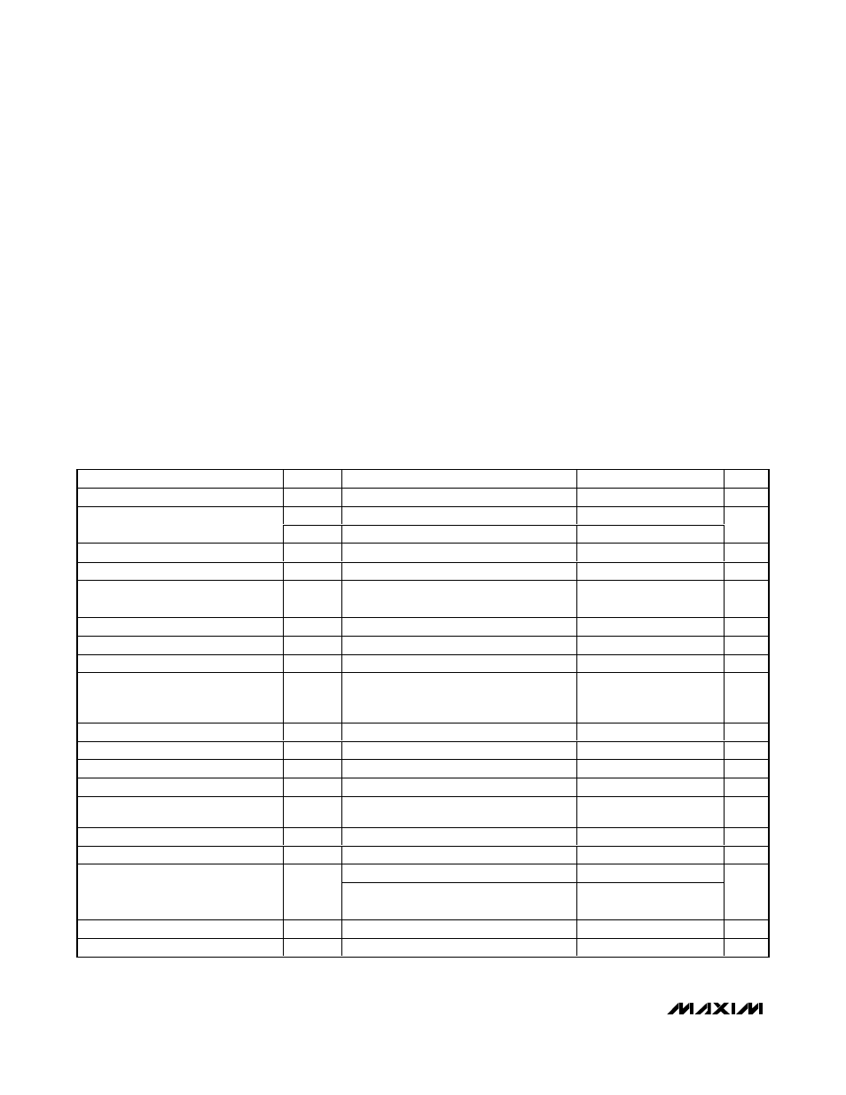
ABSOLUTE MAXIMUM RATINGS
ELECTRICAL CHARACTERISTICS
(Circuit of Figure 1, V
IN
= 12V,
SKIP_ = PGND = AGND, ON_ = V
CC
= 5V, separate mode, T
A
= 0°C to +85°C, unless otherwise
noted. Typical values are at T
A
= +25°C.)
Stresses beyond those listed under “Absolute Maximum Ratings” may cause permanent damage to the device. These are stress ratings only, and functional
operation of the device at these or any other conditions beyond those indicated in the operational sections of the specifications is not implied. Exposure to
absolute maximum rating conditions for extended periods may affect device reliability.
VDD, VCC, CSH_, CSL_ to AGND............................-0.3V to +6V
ON_,
SKIP_, PGOOD_ to AGND ..............................-0.3V to +6V
OVP_, REFIN_ to AGND ...........................................-0.3V to +6V
DTRANS to AGND ....................................................-0.3V to +6V
REF, OSC, SLEW_, CCI2 to AGND ...........-0.3V to (V
CC
+ 0.3V)
BST1, BST2 to AGND .............................................-0.3V to +36V
LX1 to BST1..............................................................-6V to +0.3V
LX2 to BST2..............................................................-6V to +0.3V
DH1 to LX1 ..............................................-0.3V to (V
BST1
+ 0.3V)
DH2 to LX2 ..............................................-0.3V to (V
BST2
+ 0.3V)
DL1, DL2 to PGND .....................................-0.3V to (V
DD
+ 0.3V)
AGND to PGND .....................................................-0.3V to +0.3V
REF Short Circuit to AGND.........................................Continuous
REF Current ......................................................................+10mA
Continuous Power Dissipation (T
A
= +70°C)
32-Pin, 5mm x 5mm, Thin QFN
(derate 21.3mW/°C above +70°C) .............................1702mW
Operating Temperature Range ...........................-40°C to +85°C
Junction Temperature ......................................................+150°C
Storage Temperature Range .............................-65°C to +150°C
Lead Temperature (soldering, 10s) .................................+300°C
PARAMETER
SYM B O L CONDITIONS
MIN
TYP
MAX
UNITS
INPUT SUPPLIES
V
IN
4
26
Input Voltage Range
V
BIAS
V
CC
, V
DD
4.5
5.5
V
V
CC
Undervoltage Lockout Threshold
V
UVLO
Rising edge, 50mV typical hysteresis
4.1
4.25
4.5
V
Quiescent Supply Current (V
CC
)
I
CC
CSL_ forced above their regulation points
1.5
2.5
mA
Quiescent Supply Current (V
DD
)
I
DD
CSL_ forced above their regulation points,
SKIP mode
< 1
5
µA
Shutdown Supply Current (V
CC
)
I
C C (S H D N)
ON1 = ON2 = GND
< 1
5
µA
Shutdown Supply Current (V
DD
)
I
D D (S H D N)
ON1 = ON2 = GND
< 1
5
µA
SMPS CONTROLLERS
Output Voltage Accuracy
V
REFIN_
-
V
CSL_
With respect to REFIN_,
REFIN_ = 0.5V to 2.5V,
SKIP_ = V
CC
or GND (Note 1)
-5
0
+5
mV
Output Voltage-Adjust Range
V
CSL_
Either SMPS (Note 2)
0.5
2.5
V
RE FIN Op er ati ng V ol tag e- Ad j ust Rang e
V
REFIN_
Either SMPS (Note 2)
0.5
2.5
V
REFINOK Threshold
Either SMPS
0.1
V
REFIN Transient Detection Threshold
5mV (typ) hysteresis
±25
mV
Combined-Mode Enabled Threshold
V
REFIN2
3
V
CC
-
1
V
CC
-
0.4
V
DC Load Regulation
Either SMPS,
SKIP_ = V
CC
, zero to full load
-0.1
%
Line Regulation Error
Either SMPS, 4V < V
IN
< 26V
0.03
%/V
R
OSC
= 143k
Ω (f
OSC
= 300kHz nominal)
-10
+10
Switching-Frequency Accuracy
(Note 3)
f
OSC
R
OSC
= 71.5k
Ω (f
OSC
= 600kHz nominal) to
432k
Ω (f
OSC
= 99kHz nominal)
-15
+15
%
Maximum Duty Factor
D
MAX
91
93
%
Minimum On-Time
t
ONMIN
(Note 4)
150
ns