3 adc converter operation, 4 voltage conversion, 5 clock selection – Rainbow Electronics T89C51AC2 User Manual
Page 82
82
T89C51AC2
Rev. B – 19-Dec-01
16.3 ADC Converter
Operation
A start of single A/D conversion is triggered by setting bit ADSST (ADCON.3).
After completion of the A/D conversion, the ADSST bit is cleared by hardware.
The end-of-conversion flag ADEOC (ADCON.4) is set when the value of conversion is
available in ADDH and ADDL, it must be cleared by software. If the bit EADC (IEN1.1) is
set, an interrupt occur when flag ADEOC is set (see Figure 39). Clear this flag for re-
arming the interrupt.
The bits SCH0 to SCH2 in ADCON register are used for the analog input channel
selection.
Table 43. Selected Analog input
16.4 Voltage Conversion
When the ADCIN is equals to VAREF the ADC converts the signal to 3FFh (full scale). If
the input voltage equals VAGND, the ADC converts it to 000h. Input voltage between
VAREF and VAGND are a straight-line linear conversion. All other voltages will result in
3FFh if greater than VAREF and 000h if less than VAGND.
Note that ADCIN should not exceed VAREF absolute maximum range! (see section
“AC-DC”)
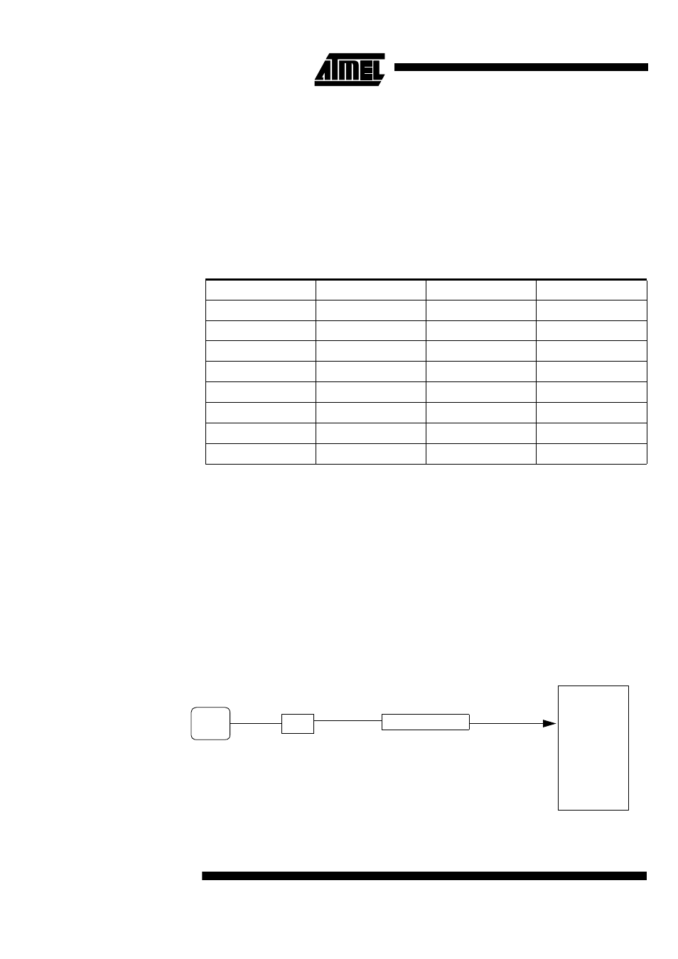
16.5 Clock Selection
The ADC clock is the same as CPU.
The maximum clock frequency for ADC is 700KHz. A prescaler is featured (ADCCLK) to
generate the ADC clock from the oscillator frequency.
Figure 38. A/D Converter clock
SCH2
SCH1
SCH0
Selected Analog input
0
0
0
AN0
0
0
1
AN1
0
1
0
AN2
0
1
1
AN3
1
0
0
AN4
1
0
1
AN5
1
1
0
AN6
1
1
1
AN7
Prescaler ADCLK
A/D
Converter
ADC Clock
CPU
CLOCK
CPU Core Clock Symbol
ч
2