Figure 5), Figure 6 – Rainbow Electronics T89C51AC2 User Manual
Page 22
22
T89C51AC2
Rev. B – 19-Dec-01
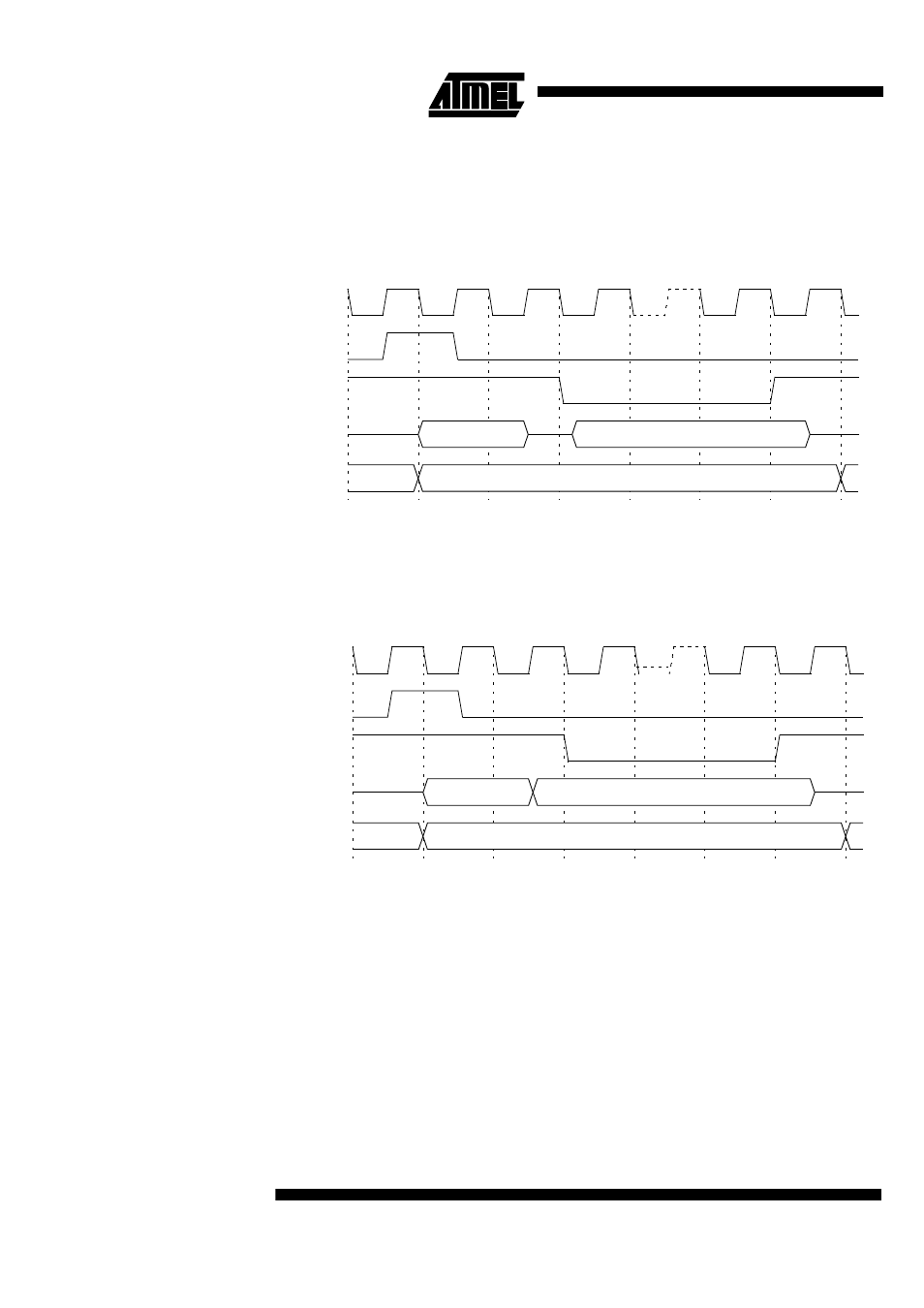
For simplicity, the accompanying figures depict the bus cycle waveforms in idealized
form and do not provide precise timing information. For bus cycle timing parameters
refer to the Section “AC Characteristics” of the T89C51AC2 datasheet.
Figure 5. External Data Read Waveforms
Notes:
1. RD# signal may be stretched using M0 bit in AUXR register.
2. When executing MOVX @Ri instruction, P2 outputs SFR content.
Figure 6. External Data Write Waveforms
Notes:
1. WR# signal may be stretched using M0 bit in AUXR register.
2. When executing MOVX @Ri instruction, P2 outputs SFR content.
ALE
P0
P2
RD#1
DPL or Ri
D7:0
DPH or P22
P2
CPU Clock
ALE
P0
P2
WR#1
DPL or Ri
D7:0
P2
CPU Clock
DPH or P22
See also other documents in the category Rainbow Electronics Sensors:
- MAX5151 (16 pages)
- MAXQ3108 (64 pages)
- MAX5661 (39 pages)
- MAX6691 (7 pages)
- MAX5362 (12 pages)
- ADC10158 (26 pages)
- MAX8922L (14 pages)
- MAX8596Z (8 pages)
- MAX7491 (18 pages)
- MAX15040 (15 pages)
- MAX5177 (16 pages)
- ADC08138 (22 pages)
- MAX5961 (42 pages)
- T89C51RD2 (86 pages)
- MAX16055 (9 pages)
- MAX6659 (17 pages)
- ADC0820 (20 pages)
- MAX6678 (19 pages)
- MAX8884Z (15 pages)
- MAX16915 (9 pages)
- MAX8620 (18 pages)
- MAX5144 (12 pages)
- MAX6670 (8 pages)
- MAX8760 (39 pages)
- W78C32C (14 pages)
- MX7533 (8 pages)
- MAX8727 (13 pages)
- MAX9053 (15 pages)
- W78C54 (16 pages)
- MAX8614B (15 pages)
- W90N740 (219 pages)
- MAX6626 (13 pages)
- ADC10738 (30 pages)
- MAX17000 (31 pages)
- MAX5051 (21 pages)
- MAXQ1004 (18 pages)
- MAX6871 (51 pages)
- MX7847 (12 pages)
- MAX6608 (6 pages)
- MAX17083 (15 pages)
- MAX6641 (17 pages)
- MAX5251 (16 pages)
- MAX6338 (8 pages)
- MAX6690 (16 pages)
- MAX8668 (18 pages)