3 port 0 and port2 – Rainbow Electronics T89C51AC2 User Manual
Page 7
7
T89C51AC2
Rev. B – 19-Dec-01
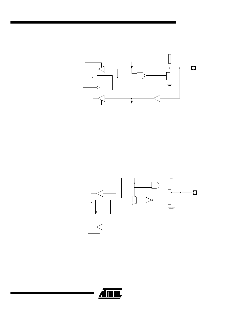
Figure 1. Port 1, Port 3 and Port 4 Structure
Note:
The internal pull-up can be disabled on P1 when analog function is selected.
4.3 Port 0 and Port2
Ports 0 and 2 are used for general-purpose I/O or as the external address/data bus. Port
0, shown in Figure 3, differs from the other Ports in not having internal pull-ups. Figure 3
shows the structure of Port 2. An external source can pull a Port 2 pin low.
To use a pin for general-purpose output, set or clear the corresponding bit in the Px reg-
ister (x=0 or 2). To use a pin for general purpose input, set the bit in the Px register to
turn off the output driver FET.
Figure 2. Port 0 Structure
Notes:
1. Port 0 is precluded from use as general purpose I/O Ports when used as
address/data bus drivers.
2. Port 0 internal strong pull-ups assist the logic-one output for memory bus cycles only.
Except for these bus cycles, the pull-up FET is off, Port 0 outputs are open-drain.
D
CL
Q
P1.X
LATCH
INTERNAL
WRITE
TO
LATCH
READ
PIN
READ
LATCH
P1.x
P3.X
P4.X
ALTERNATE
OUTPUT
FUNCTION
VCC
INTERNAL
PULL-UP (1)
ALTERNATE
INPUT
FUNCTION
P3.x
P4.x
BUS
D
Q
P0.X
LATCH
INTERNAL
WRITE
TO
LATCH
READ
PIN
READ
LATCH
0
1
P0.x (1)
ADDRESS LOW/
DATA
CONTROL
VDD
BUS
(2)