Program/code memory, 1 external code memory access – Rainbow Electronics T89C51AC2 User Manual
Page 29
29
T89C51AC2
Rev. B – 19-Dec-01
9. Program/Code
Memory
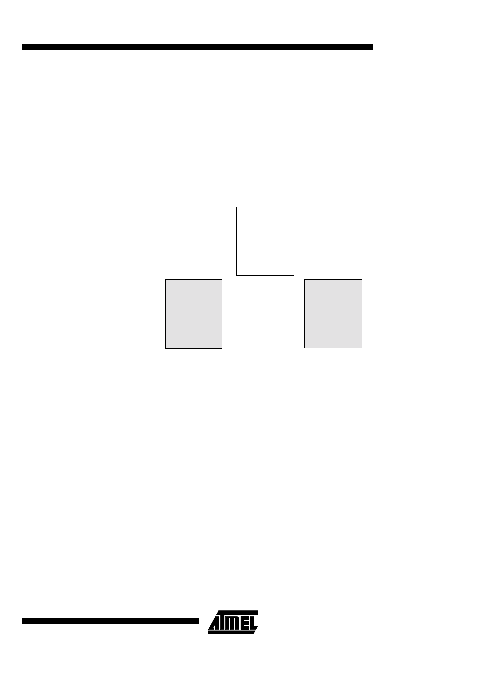
The T89C51AC2 implement 32 Kbytes of on-chip program/code memory. Figure 8
shows the partitioning of internal and external program/code memory spaces depending
on the product.
The FLASH memory increases EPROM and ROM functionality by in-circuit electrical
erasure and programming. Thanks to the internal charge pump, the high voltage needed
for programming or erasing FLASH cells is generated on-chip using the standard VDD
voltage. Thus, the FLASH Memory can be programmed using only one voltage and
allows In-System Programming commonly known as ISP. Hardware programming mode
is also available using specific programming tool.
Figure 8. Program/Code Memory Organization
Note:
If the program executes exclusively from on-chip code memory (not from external mem-
ory), beware of executing code from the upper byte of on-chip memory (7FFFh) and
thereby disrupt I/O Ports 0 and 2 due to external prefetch. Fetching code constant from
this location does not affect Ports 0 and 2.
9.1 External Code
Memory Access
9.1.1 Memory Interface
The external memory interface comprises the external bus (port 0 and port 2) as well as
the bus control signals (PSEN#, and ALE).
Figure 9 shows the structure of the external address bus. P0 carries address A7:0 while
P2 carries address A15:8. Data D7:0 is multiplexed with A7:0 on P0. Table 7 describes
the external memory interface signals.
0000h
32 Kbytes
7FFFh
internal
0000h
7FFFh
FFFFh
8000h
FLASH
32 Kbytes
external
memory
32 Kbytes
external
memory
EA = 0
EA = 1