2 flash memory architecture – Rainbow Electronics T89C51AC2 User Manual
Page 31
31
T89C51AC2
Rev. B – 19-Dec-01
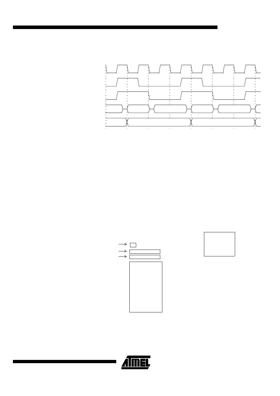
Figure 10. External Code Fetch Waveforms
9.2 FLASH Memory
Architecture
T89C51AC2 features two on-chip flash memories:
•
Flash memory FM0:
containing 32 Kbytes of program memory (user space) organized into 128 byte
pages,
•
Flash memory FM1:
2 Kbytes for boot loader and Application Programming Interfaces (API).
The FM0 can be program by both parallel programming and Serial In-System Program-
ming (ISP) whereas FM1 supports only parallel programming by programmers. The ISP
mode is detailed in the "In-System Programming" section.
All Read/Write access operations on FLASH Memory by user application are managed
by a set of API described in the "In-System Programming" section.
Figure 11. Flash memory architecture
ALE
P0
P2
PSEN#
PCL
PCH
PCH
PCL
D7:0
D7:0
PCH
D7:0
CPU Clock
7FFFh
32 Kbytes
Flash memory
FM0
0000h
Hardware Security (1 byte)
Column Latches (128 bytes)
user space
Extra Row (128 bytes)
2 Kbytes
Flash memory
FM1
boot space
FFFFh
F800h
FM1 mapped between FFFFh and
F800h when bit ENBOOT is set in
AUXR1 register