Combination mode 12: burst modulation 2, Combination mode 13: fsk modulation – Rainbow Electronics T48C862-R4 User Manual
Page 89

89
T48C862-R4
4551B–4BMCU–02/03
Combination Mode 12:
Burst Modulation 2
SSI mode 1:
8-bit shift register internal data output (SO) to the Timer 3
Timer 2 output mode 2:
8-bit compare counter and 4-bit prescaler
Timer 2 output mode 1/6: Timer 2 compare match toggles (TOG2) to the SSI
Timer 3 mode 7:
Carrier frequency burst modulation controlled by the internal
output (SO) of SSI
The Timer 3 counter is driven by an internal or external clock source. Its compare- and
compare mode registers must be programmed to generate the carrier frequency with
the output toggle flip-flop (M3). The internal data output (SO) of the SSI is used to
enable and disable the Timer 3 output. The SSI can be supplied with the toggle signal of
Timer 2.
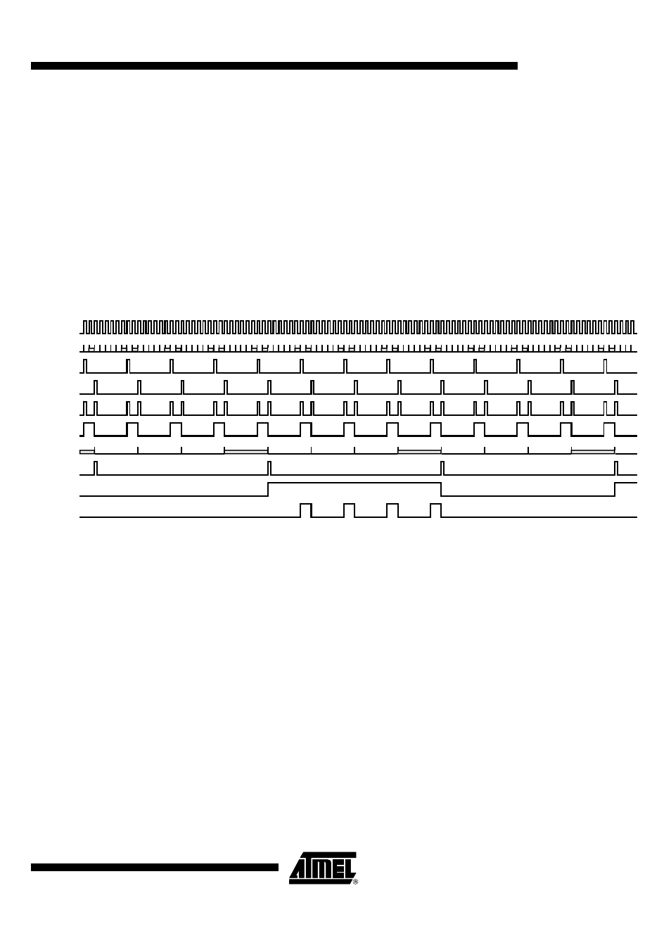
Figure 89.
Burst Modulation 2
Combination Mode 13:
FSK Modulation
SSI mode 1:
8-bit shift register internal data output (SO) to the Timer 3
Timer 2 output mode 3:
8-bit compare counter and 4-bit prescaler
Timer 2 output mode 1/6: Timer 2 4-bit compare match signal (POUT) to the SSI
Timer 3 mode 8:
FSK modulation with shift register data output (SO)
The two compare registers are used to generate two different time intervals. The SSI
data output selects which compare register is used for the output frequency generation.
A "0" level at the SSI data output enables the compare register 1 and a "1" level enables
the compare register 2. The compare- and compare mode registers must be pro-
grammed to generate the two frequencies via the output toggle flip-flop. The SSI can be
supplied with the toggle signal of Timer 2 or any other clock source. The Timer 3 counter
is driven by an internal or external clock source.
0 1 0 1 2 3 4 5 0 1 0 1 2 3 4 5 0 1 0 1 2 3 4 5 0 1 0 1
5 0 1 0 1
5 0 1 0 1
5 0 1 0 1
5 0 1 0 1
5 0 1 0 1
5 0 1 0 1
5 0 1 0 1
5 0 1 0 1
5 0 1 0 1
3
0
1
2
3
3
0
1
3
2
CL3
Counter 3
CM31
CM32
TOG3
M3
Counter 2/2
TOG2
SO
T3O
