Reset function, Marc4 architecture general description, Components of marc4 core – Rainbow Electronics T48C862-R4 User Manual
Page 14: Program memory, Marc4 core

14
T48C862-R4
4551B–4BMCU–02/03
Reset Function
During each reset (power-on or brown-out), the I/O configuration is deleted and
reloaded with the data from the configuration memory. This leads to a slightly different
behavior compared to the ROM versions. Both devices switch their I/Os to input during
reset but the ROM part has the mask selected pull-up or pull-down resistors active while
the MTP has them removed until the download is finished.
MARC4 Architecture
General Description
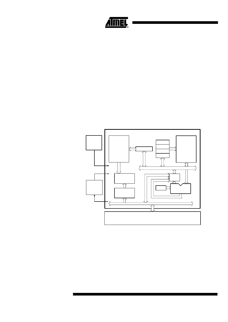
The microcontroller consists of an advanced stack-based, 4-bit CPU core and on-chip
peripherals. The CPU is based on the Harvard architecture with physically separated
program memory (ROM) and data memory (RAM). Three independent buses, the
instruction bus, the memory bus and the I/O bus, are used for parallel communication
between ROM, RAM and peripherals. This enhances program execution speed by
allowing both instruction prefetching, and a simultaneous communication to the on-chip
peripheral circuitry. The extremely powerful integrated interrupt controller with associ-
ated eight prioritized interrupt levels supports fast and efficient processing of hardware
events. The microcontroller is designed for the high-level programming language
qFORTH. The core includes both an expression and a return stack. This architecture
enables high-level language programming without any loss of efficiency or code density.
Figure 9.
MARC4 Core
Components of
MARC4 Core
The core contains ROM, RAM, ALU, program counter, RAM address registers, instruc-
tion decoder and interrupt controller. The following sections describe each functional
block in more detail.
Program Memory
The program memory (EEPROM) is programmable with the customer application
program during the fabrication of the microcontroller. The EEPROM is addressed by a
12-bit wide program counter, thus predefining a maximum program bank size of
4-Kbytes. The lowest user program memory address segment is taken up by a
512 bytes Zero page which contains predefined start addresses for interrupt service rou-
tines and special subroutines accessible with single byte instructions (SCALL).
Instruction
decoder
CCR
TOS
ALU
RAM
RP
X
Y
Program
256 x 4-bit
MARC4 CORE
Clock
Reset
Sleep
Memory bus
I/O bus
Instruction
bus
Reset
System
clock
Interrupt
controller
On-chip peripheral modules
memory
SP
PC
