Electrical characteristics (continued) – Rainbow Electronics MAX17008 User Manual
Page 6
MAX17007A/MAX17008
Dual and Combinable QPWM Graphics
Core Controllers for Notebook Computers
6
_______________________________________________________________________________________
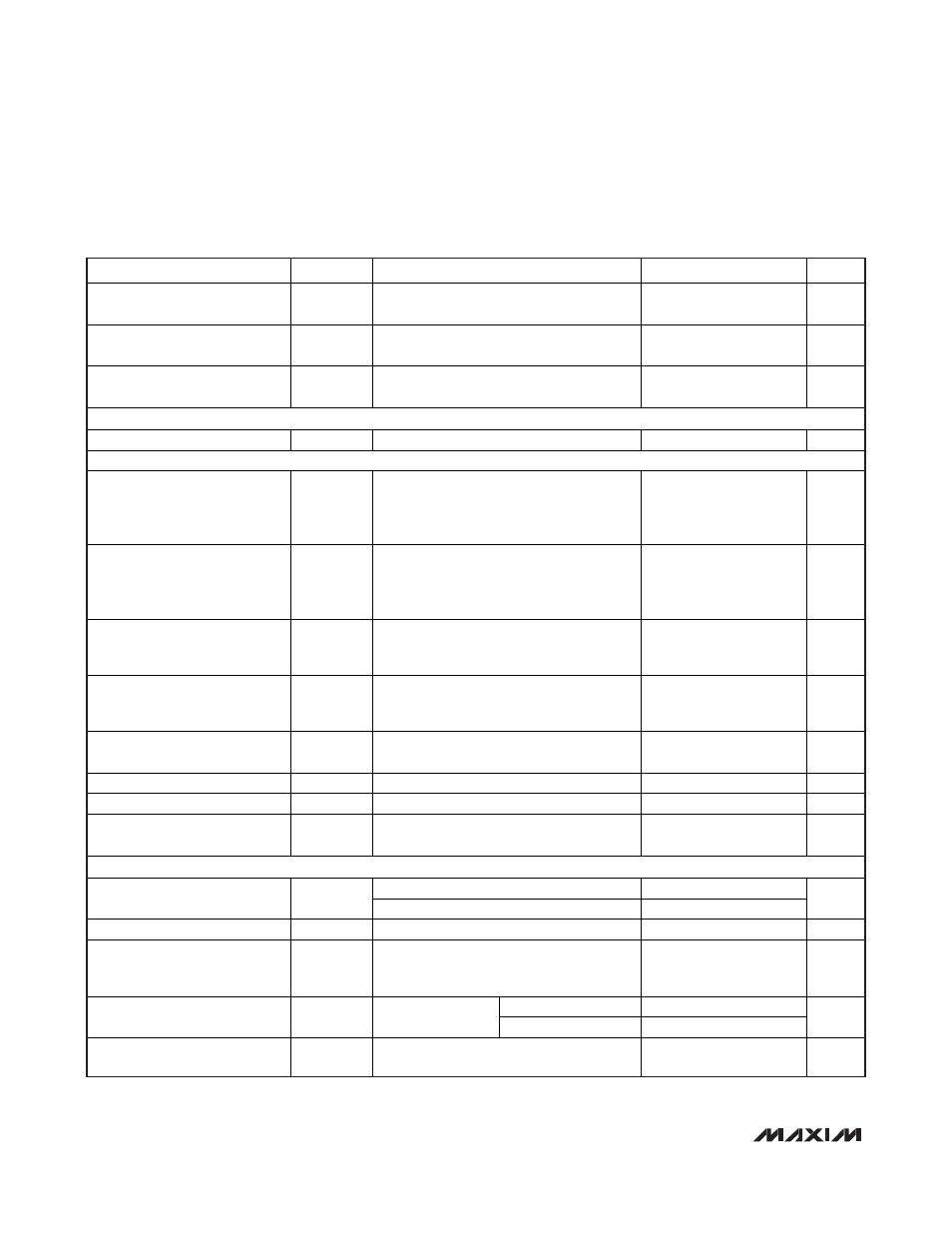
ELECTRICAL CHARACTERISTICS (continued)
(V
IN
= 12V, V
DD
= V
CC
= V
EN1
= V
EN2
= 5V, V
REFIN1
= 2V, SKIP = GND, T
A
= -40°C to +105°C, unless otherwise noted.) (Note 4)
PARAMETER
SYMBOL
CONDITIONS
MIN
MAX
UNITS
REFIN1 Dual-Mode
Switchover Threshold
3.75
V
CC
-
0.4
V
SMPS1 Voltage Accuracy
V
CSL1
Measured at CSL1, REFIN1 = V
CC;
V
IN
= 2V to 26V,
SKIP = V
CC
(Note 2)
1.039 1.061 V
SMPS2 Voltage Accuracy
V
CSL2
Measured at CSL2, FB2 = REF;
V
IN
= 2V to 26V,
SKIP = V
CC
(Note 2)
1.485 1.515 V
INTERNAL REFERENCE
Reference Voltage
V
REF
V
DD
= 4.5V to 5.5V
1.985
2.015
V
FAULT DETECTION
SMPS1 Overvoltage Trip
Threshold and PGOOD1
Upper Threshold
(MAX17007A Only)
V
OVP1
,
V
PG1_H
With respect to the internal target voltage
(error comparator threshold); rising edge;
hysteresis = 50mV
260 340
mV
SMPS2 Overvoltage Trip
Threshold and PGOOD2
Upper Threshold
(MAX17007A Only)
V
OVP2
,
V
PG2_H
With respect to the internal target voltage
0.7V (error comparator threshold);
hysteresis = 50mV
120 180
mV
SMPS1 Undervoltage Protection
Trip Threshold and Lower
PGOOD1 Threshold
V
UVP1
,
V
PG1_L
With respect to the internal target voltage
(error comparator threshold) falling edge;
hysteresis = 50mV
-240 -160
mV
SMPS2 Undervoltage Protection
Trip Threshold and Lower
PGOOD2 Threshold
V
UVP2
,
V
PG2_L
With respect to the internal target voltage
0.7V (error comparator threshold)
falling edge; hysteresis = 50mV
-130 -70 mV
Output Undervoltage Fault
Propagation Delay
t
UVP
REFIN1/FB2 forced 25mV below trip
threshold
90 360
μs
PGOOD_ Propagation Delay
t
PGOOD
Startup delay from regulation
90
360
μs
PGOOD_ Output Low Voltage
I
SINK
= 3mA
0.4
V
V
CC
Undervoltage Lockout
Threshold
V
UVLO(VCC)
Rising edge, PWM disabled below this level;
hysteresis = 100mV
3.8 4.45 V
CURRENT LIMIT
CSH1, CSH2
0
2.3
Current-Sense Input Range
CSL1, CSL2
0
2.3
V
Current-Limit Threshold (Fixed)
V
CSLIMIT
V
CSH_
- V
CSL_
, ILIM1 = ILIM2 = REF
27
33
mV
Ultrasonic Frequency
SKIP = OPEN (3.3V);
V
CSL1
= V
REFIN1
+ 50mV;
V
CSL2
= V
FB2
+ 50mV
18 kHz
V
CSL1
= V
REF1
+ 50mV
22
46
Ultrasonic Current-Limit
Threshold
SKIP = OPEN (3.3V)
V
CSL2
= V
FB2
+ 50mV
18
46
mV
Current-Balance Amplifier (GMI)
Offset
[V(CSH1,CSL1) - V(CSH2,CSL2)] at I
CCI
= 0
-3
+3
mV