Rainbow Electronics MAX17008 User Manual
Page 34
MAX17007A/MAX17008
3) Group the gate-drive components (BST capacitors,
V
DD
bypass capacitor) together near the controller IC.
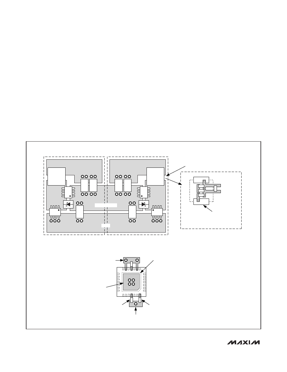
4) Make the DC-DC controller ground connections as
shown in Figures 1 and 2. This diagram can be
viewed as having four separate ground planes: I/O
ground, where all the high-power components go;
the power ground plane, where the PGND pin and
V
DD
bypass capacitor go; the master’s analog
ground plane where sensitive analog components,
the master’s GND pin, and V
CC
bypass capacitor
go; and the slave’s analog ground plane where the
slave’s GND pin and V
CC
bypass capacitor go. The
master’s GND plane must meet the PGND plane
only at a single point directly beneath the IC.
Similarly, the slave’s GND plane must meet the
PGND plane only at a single point directly beneath
the IC. The respective master and slave ground
planes should connect to the high-power output
ground with a short metal trace from PGND to the
source of the low-side MOSFET (the middle of the
star ground). This point must also be very close to
the output capacitor ground terminal.
5) Connect the output power planes (V
OUT
and sys-
tem ground planes) directly to the output filter
capacitor positive and negative terminals with multi-
ple vias. Place the entire DC-DC converter circuit as
close to the load as is practical. See Figure 15.
Dual and Combinable QPWM Graphics
Core Controllers for Notebook Computers
34
______________________________________________________________________________________
OUTPUT 1
SMPS1
C
OUT1
C
OUT1
C
OUT2
C
OUT2
C
IN1
C
IN2
SMPS2
OUTPUT 2
KELVIN SENSE VIAS
UNDER THE INDUCTOR
(SEE MAX17007A EVALUATION KIT)
VIA TO POWER
GROUND
V
CC
BYPASS
CAPACITOR
REF BYPASS
CAPACITOR
X-RAY VIEW.
IC MOUNTED
ON BOTTOM
SIDE OF PCB.
IC LAYOUT
CONNECT GND AND PGND THE
CONTROLLER AT ONE POINT
ONLY AS SHOWN
CONNECT THE
EXPOSED PAD TO
ANALOG GND
VIA TO ANALOG
GROUND
POWER STAGE LAYOUT (TOP SIDE OF PCB)
INDUCTOR
L1
INDUCTOR
L2
INPUT
POWER GROUND
+
INDUCTOR DCR SENSING
KELVIN SENSE VIAS TO
INDUCTOR PAD
CSL
CSH
Figure 15. PCB Layout Example