Rainbow Electronics MAX17008 User Manual
Page 2
MAX17007A/MAX17008
Dual and Combinable QPWM Graphics
Core Controllers for Notebook Computers
2
_______________________________________________________________________________________
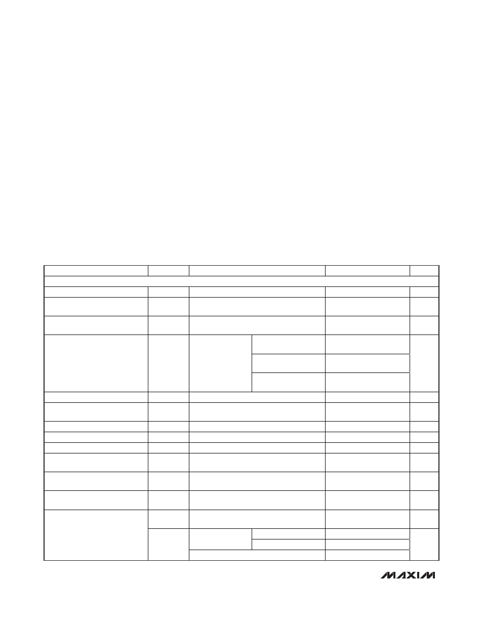
ABSOLUTE MAXIMUM RATINGS
ELECTRICAL CHARACTERISTICS
(V
IN
= 12V, V
DD
= V
CC
= V
EN1
= V
EN2
= 5V, V
REFIN1
= 2V, SKIP = GND, T
A
= 0 to +85°C, unless otherwise noted. Typical values are
at T
A
= +25°C.)
Stresses beyond those listed under “Absolute Maximum Ratings” may cause permanent damage to the device. These are stress ratings only, and functional
operation of the device at these or any other conditions beyond those indicated in the operational sections of the specifications is not implied. Exposure to
absolute maximum rating conditions for extended periods may affect device reliability.
BST1, BST2 to GND ...............................................-0.3V to +34V
BST1, BST2 to V
DD
.................................................-0.3V to +28V
TON1, TON2 to GND..............................................-0.3V to +28V
V
DD
to GND ..............................................................-0.3V to +6V
V
DD
to V
CC
............................................................-0.3V to +0.3V
LX1 to BST1..............................................................-6V to +0.3V
LX2 to BST2..............................................................-6V to +0.3V
DH1 to LX1 ..............................................-0.3V to (V
BST1
+ 0.3V)
DH2 to LX2 ..............................................-0.3V to (V
BST2
+ 0.3V)
ILIM1, ILIM2, REF to GND ..........................-0.3V to (V
CC
+ 0.3V)
CSH1, CSH2, CSL1, CSL2, FB2, REFIN1 to GND....-0.3V to +6V
EN1, EN2, SKIP, PGOOD1, PGOOD2 to GND.........-0.3V to +6V
DL1 to GND ................................................-0.3V to (V
DD
+ 0.3V)
DL2 to PGND..............................................-0.3V to (V
DD
+ 0.3V)
PGND to GND ......................................................-0.3V to + 0.3V
REF Short Circuit to GND ...........................................Continuous
Continuous Power Dissipation (T
A
= +70°C)
28-Pin TQFN T2844-1
(derate 20.8mW/°C above +70°C) ............................1667mW
Extended Operating Temperature Range .........-40°C to +105°C
Junction Temperature ......................................................+150°C
Storage Temperature Range .............................-65°C to +150°C
Lead Temperature (soldering, 10s) .................................+300°C
PARAMETER
SYMBOL
CONDITIONS
MIN
TYP
MAX
UNITS
PWM CONTROLLER
Input Voltage Range
V
IN
4.5
26
V
Quiescent Supply Current
(V
DD
, V
CC
)
I
DD
+ I
CC
Output forced above regulation voltage,
V
EN1
= V
EN2
= 5V
1.7
2.5
mA
Shutdown Supply Current
(V
DD
, V
CC
)
I
SHDN
EN1 = EN2 = GND, T
A
= +25°C
0.1
5
μA
R
TON1
= R
TON2
=
97.5k
(600kHz)
142
(-15%)
174
194
(+15%)
R
TON1
= R
TON2
=
200k
(300kHz)
305
(-10%)
336
368
(+10%)
On-Time (Note 1)
t
ON1
, t
ON2
V
IN
= 12V,
V
CSL1
= V
CSL2
=
V
CCI
= 1.2V,
separate or
combined mode
R
TON1
= R
TON2
=
302.5k
(200kHz)
425
(-15%)
500
575
(+15%)
ns
Minimum Off-Time
t
OFF(MIN)
(Note
1)
250
400
ns
TON1, TON2, Shutdown Supply
Current
I
TON1
,
I
TON2
EN1 = EN2 = GND, V
TON1
= V
TON2
= 26V,
V
DD
= 0 or 5V, T
A
= +25°C
0.01 1 μA
REFIN1 Voltage Range
V
REFIN1
(Note 2)
0
V
REF
V
FB2 Regulation Voltage
V
FB2
Adjustable mode
0.7
V
FB2 Input Voltage Range
Preset mode
1.7
2.3
V
FB2 Combined-Mode Threshold
Combined mode
3.8
V
CC
-
1V
V
CC
-
0.4
V
REFIN1 Dual Mode™
Switchover Threshold
3.8
V
CC
-
1V
V
CC
-
0.4
V
REFIN1, FB2 Bias Current
I
REFIN1
,
I
FB2
REFIN1 = 0.5V to 2V;
V
FB2
= 0.7V, T
A
= +25°C
-0.1 +0.1
μA
V
CSL1
Measured at CSL1, REFIN1 = V
CC
,
V
IN
= 2V to 26V,
SKIP = V
CC
(Note 2)
1.043 1.05 1.057 V
T
A
= +25°C
-12
+12
REFIN1 = 500mV,
SKIP = V
CC
T
A
= 0°C to +85°C
-20
+20
SMPS1 Voltage Accuracy
V
CSL1
-
V
REFIN1
REFIN1 = 2V,
SKIP = V
CC
-20
+20
mV
Dual Mode is a trademark of Maxim Integrated Products, Inc.