Electrical characteristics (continued) – Rainbow Electronics MAX17008 User Manual
Page 3
MAX17007A/MAX17008
Dual and Combinable QPWM Graphics
Core Controllers for Notebook Computers
_______________________________________________________________________________________
3
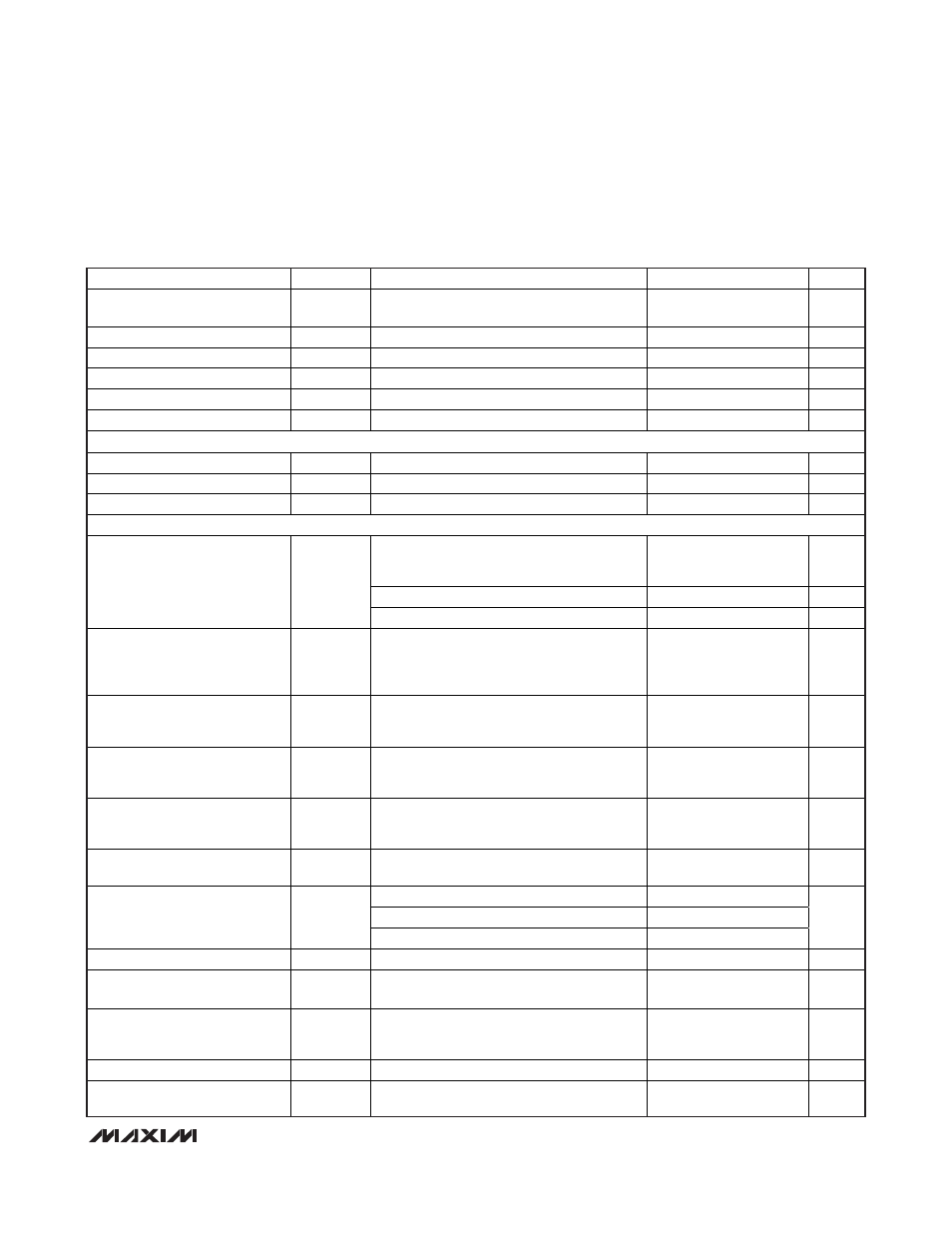
PARAMETER SYMBOL
CONDITIONS
MIN
TYP
MAX
UNITS
SMPS2 Voltage Accuracy
V
CSL2
Measured at CSL2, FB2 = REF,
V
IN
= 2V to 26V,
SKIP = V
CC
1.489 1.5 1.511 V
Load Regulation Error
I
LOAD
= 0 to full load,
SKIP = V
CC
(Note 3)
0.1
%
Line Regulation Error
V
DD
= 4.5V to 5.5V, V
IN
= 4.5V to 26V (Note 3)
0.25
%
CSL1 Soft-Start/-Stop Slew Rate
SR
SS1
Rising/falling edge on EN1
1.25
mV/μs
FB2 Soft-Start/-Stop Slew Rate
SR
SS2
Rising/falling edge on EN2
0.63
mV/μs
Dynamic REFIN1 Slew Rate
SR
DYN
Rising edge on REFIN1
11.4
mV/μs
INTERNAL REFERENCE
Reference Voltage
V
REF
V
DD
= 4.5V to 5.5V
1.990
2.000
2.010
V
Reference Lockout Voltage
V
REF(UVLO)
Rising edge, hysteresis = 230mV
1.8
V
Reference Load Regulation
I
REF
= -10μA to +100μA
1.980
2.015
mV
FAULT DETECTION
With respect to the internal target voltage
(error comparator threshold); rising edge;
hysteresis = 50mV
260 300 340 mV
Dynamic transition
V
REF
+ 0.30
V
SMPS1 Overvoltage Trip
Threshold and PGOOD1 Upper
Threshold
(MAX17007A Only)
V
OVP1
,
V
PG1_H
Minimum OVP threshold
0.7
V
SMPS2 Adjustable Mode
Overvoltage Trip Threshold and
PGOOD2 Upper Threshold
(MAX17007A Only)
V
OVP2
,
V
PG2_H
With respect to the internal target voltage
0.7V (error comparator threshold);
hysteresis = 50mV
120 150 180 mV
Output Overvoltage Fault
Propagation Delay
(MAX17007A Only)
t
OVP
CSL1/FB2 forced 25mV above trip threshold
5
μs
SMPS1 Undervoltage Protection
Trip Threshold and Lower
PGOOD1 Threshold
V
UVP1
,
V
PG1_L
With respect to the internal target voltage
(error comparator threshold); falling edge;
hysteresis = 50mV
-240 -200 -160 mV
SMPS2 Undervoltage Protection
Trip Threshold and Lower
PGOOD2 Threshold
V
UVP2
,
V
PG2_L
With respect to the internal target voltage
0.7V (error comparator threshold);
falling edge; hysteresis = 50mV
-130 -100 -70
mV
Output Undervoltage Fault
Propagation Delay
t
UVP
CSL1/FB2 forced 25mV below trip threshold
90
205
360
μs
UVP falling edge, 25mV overdrive
5
OVP rising edge, 25mV overdrive
5
PGOOD_ Propagation Delay
t
PGOOD
Startup delay from regulation
90
205
360
μs
PGOOD_ Output Low Voltage
I
SINK
= 3mA
0.4
V
PGOOD_ Leakage Current
I
PGOOD
CSL1 = REFIN1, FB2 = 0.7V (PGOOD_ high
impedance), PGOOD_ forced to 5V, T
A
= +25°C
1
μA
Dynamic REFIN1 Transition
Fault-Blanking Threshold
Fault blanking initiated; REFIN1 deviation
from the internal target voltage (error
comparator threshold); hysteresis = 10mV
±50 mV
Thermal-Shutdown Threshold
T
SHDN
Hysteresis = 15°C (Note 3)
160
°C
V
CC
Undervoltage Lockout
Threshold
V
UVLO(VCC)
Rising edge, PWM disabled below this level,
hysteresis = 100mV
3.95 4.20 4.45
V
ELECTRICAL CHARACTERISTICS (continued)
(V
IN
= 12V, V
DD
= V
CC
= V
EN1
= V
EN2
= 5V, V
REFIN1
= 2V, SKIP = GND, T
A
= 0 to +85°C, unless otherwise noted. Typical values are
at T
A
= +25°C.)