Rainbow Electronics MAX17008 User Manual
Page 11
MAX17007A/MAX17008
Dual and Combinable QPWM Graphics
Core Controllers for Notebook Computers
______________________________________________________________________________________
11
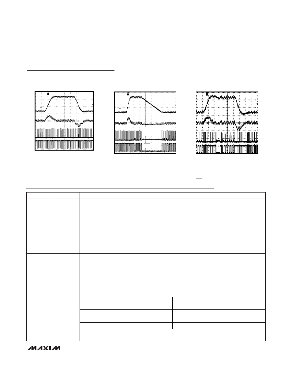
DYNAMIC OUTPUT VOLTAGE
TRANSITION (PWM MODE)
MAX17007A/8 toc26
20
μs/div
A
B
C
D
I
OUT1
= 2A
REFIN1 = 1V
TO 1.2V TO 1V
1.2V
1V
0
2A
12V
0
5V
A. V
OUT1
, 100mV/div
B. I
LX1
, 10A/div
C. LX1, 10V/div
D. DL1, 5V/div
SKIP = 5V
DYNAMIC OUTPUT VOLTAGE
TRANSITION (SKIP MODE)
MAX17007A/8 toc27
40
μs/div
A
B
C
D
I
OUT1
= 1A
1.2V
1V
0
0
12V
0
5V
A. V
OUT1
, 100mV/div
B. I
LX1
, 10A/div
C. LX1, 10V/div
D. DL1, 5V/div
REFIN1 = 1V
TO 1.2V TO 1V
SKIP = GND
DYNAMIC OUTPUT-VOLTAGE TRANSITION
(SKIP MODE-FORCED TRANSITION)
MAX17007A/8 toc28
20
μs/div
A
B
C
D
1.2V
1V
0
0
12V
0
5V
A. V
OUT1
, 100mV/div
B. I
LX2
, 10A/div
I
OUT1
= 1A
REFIN1 = 1V TO 1.2V TO 1V
SKIP = REF
C. LX1, 10V/div
D. DL1, 5V/div
I
OUT1
= 3A
Pin Description
Typical Operating Characteristics (continued)
(Circuit of Figure 1, V
IN
= 12V, V
DD
= 5V, SKIP = GND, T
A
= +25°C, unless otherwise noted.)
PIN
NAME
FUNCTION
1 REF
2V Reference Voltage Output. Bypass REF to GND with a 2.2nF ceramic capacitor. The reference
can source up to 100μA. Loading REF degrades output-voltage accuracy according to the REF
load regulation error (see theTypical Operating Characteristics). The reference shuts down when
both EN1 and EN2 are low.
2 ILIM1
This four-level input determines the CSH1 to CSL1 current limit for SMPS1:
V
CC
(5V) = 60mV current limit
Open (3.3V) = 45mV current limit
REF (2V) = 30mV current limit
GND = 15mV current limit
In combined mode, ILIM1 sets the current-limit threshold for both sides.
This four-level input determines the CSH2 to CSL2 current limit for SMPS2:
V
CC
(5V) = 60mV current limit
Open (3.3V) = 45mV current limit
REF (2V) = 30mV current limit
GND = 15mV current limit
In combined mode, ILIM2 is the current balance integrator (CCI) output pin. Connect a capacitor
(C
CCI
) between CCI and the output. The CCI capacitor value depends on the ILIM1 setting based
on the following table:
ILIM1
C
CCI
at ILIM2 (pF)
V
CC
(5V)
120
Open (3.3V)
180
REF (2V)
220
3
ILIM2
(CCI)
GND 470
4 V
CC
5V Analog Supply Input. Bypass V
CC
from V
DD
using a 10
resistor, and to analog ground using a
1μF ceramic capacitor.