Rainbow Electronics MAX17008 User Manual
Page 18
+5V Bias Supply (V
CC
, V
DD
)
The MAX17007A/MAX17008 require an external 5V bias
supply in addition to the battery. Typically, this 5V bias
supply is the notebook’s 95%-efficient 5V system sup-
ply. Keeping the bias supply external to the IC improves
efficiency and eliminates the cost associated with the 5V
linear regulator that would otherwise be needed to sup-
ply the PWM circuit and gate drivers. If stand-alone
capability is needed, the 5V supply can be generated
with an external linear regulator such as the MAX1615.
The 5V bias supply powers both the PWM controllers
and internal gate-drive power, so the maximum current
drawn depends on the external MOSFET’s gate capaci-
tance, and the selected switching frequency:
I
BIAS
= I
Q
+ f
SW1
Q
G(SMPS1)
+ f
SW2
Q
G(SMPS2)
= 4mA to 40mA (typ)
Bypass V
CC
with a 1μF or greater ceramic capacitor to
the analog ground. Bypass V
DD
with a 2.2μF or greater
ceramic capacitor to the power ground. V
CC
and V
DD
should be separated with a 10
Ω resistor (Figure 1).
2V Reference
The 2V reference is accurate to ±1% over temperature
and load, making REF useful as a precision system ref-
erence. Bypass REF to GND with a 2.2nF. The refer-
ence sources up to 100μA and sinks 10μA to support
external loads.
Combined-Mode Operation (FB2 = V
CC
)
Combined-mode operation allows the MAX17007A/
MAX17008 to support even higher output currents by
sharing the load current between two phases, distribut-
ing the power dissipation over several power compo-
nents to improve the efficiency. The MAX17007A/
MAX17008 are configured in combined mode by con-
necting FB2 to V
CC
. See Figure 2 for the combined-
mode standard application circuit.
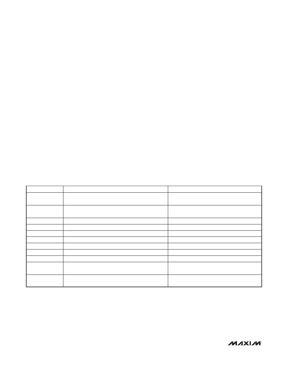
Table 3 lists the pin function differences between com-
bined mode and separate mode. See the
Pin Description
for additional details.
MAX17007A/MAX17008
Dual and Combinable QPWM Graphics
Core Controllers for Notebook Computers
18
______________________________________________________________________________________
PIN
COMBINED MODE
SEPARATE MODE
FB2
Connect to V
CC
to configure MAX17007A/MAX17008 for
combined-mode operation
Connect to REF for preset 1.5V, or use a resistor-
divider to set the SMPS2 output voltage
REFIN1
Sets the combined output voltage—dynamic, fixed, and
preset voltages supported
Sets the SMPS1 output voltage—dynamic, fixed,
and preset voltages supported
EN1
Enables/disables combined output
Enables/disables SMPS1
EN2
Not used; connect to GND
Enables/disables SMPS2
PGOOD1
Power-good indicator for combined output voltage
Power-good indicator for SMPS1
PGOOD2
Not used; can be left open
Power-good indicator for SMPS2
TON1
Sets the per-phase switching frequency for both SMPSs
Sets the switching frequency for SMPS1
TON2
Not used; leave open
Sets the switching frequency for SMPS2
ILIM1
Sets the per-phase current limit for both SMPSs
Sets SMPS1 current limit
ILIM2 (CCI)
Current-balance integrator output; connect a capacitor
from CCI to the output
Sets SMPS2 current limit
SKIP
Only three distinct modes of operation; ultrasonic mode
not supported
Supports all four modes of operation
Table 3. Pin Function in Combined and Separate Modes