Smps detailed description – Rainbow Electronics MAX17008 User Manual
Page 19
MAX17007A/MAX17008
Dual and Combinable QPWM Graphics
Core Controllers for Notebook Computers
______________________________________________________________________________________
19
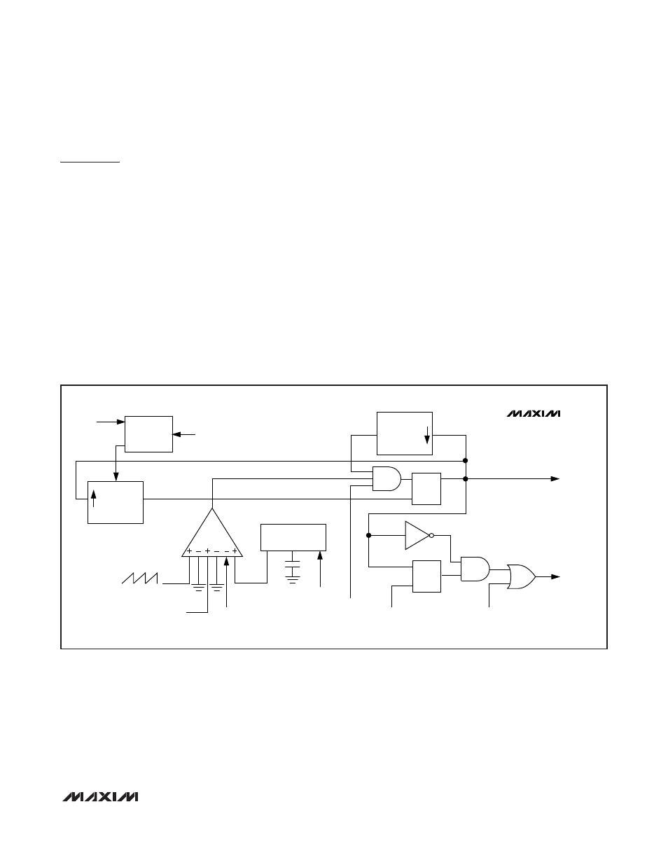
SMPS Detailed Description
Free-Running Constant-On-Time PWM
Controller with Input Feed-Forward
The Quick-PWM control architecture is a pseudo-fixed-
frequency, constant-on-time, current-mode regulator
with voltage feed-forward. This architecture relies on
the output filter capacitor’s ESR to act as a current-
sense resistor, so the output ripple voltage provides the
PWM ramp signal. The control algorithm is simple: the
high-side switch on-time is determined solely by a one-
shot whose pulse width is inversely proportional to input
voltage and directly proportional to output voltage.
Another one-shot sets a minimum off-time (150ns typ).
The on-time one-shot is triggered if the error compara-
tor is low, the low-side switch current is below the valley
current-limit threshold, and the minimum off-time one-
shot has timed out. Figure 4 is the PWM controller block
diagram.
On-Time One-Shot
The heart of the PWM core is the one-shot that sets the
high-side switch on-time. This fast, low-jitter, adjustable
one-shot includes circuitry that varies the on-time in
response to battery and output voltage. In independent
mode, the high-side switch on-time is inversely propor-
tional to the battery voltage as sensed by the TON1 and
TON2 inputs, and proportional to the voltages on CSL1
and CSL2 pins:
SMPS1 On-Time t
ON1
= T
SW1
(V
CSL1
/V
IN
)
SMPS2 On-Time t
ON2
= T
SW2
(V
CSL2
/V
IN
)
where T
SW1
(switching period of SMPS1) is set by the
resistance between TON1 and V
IN
, T
SW2
is set by the
resistance between TON2 and V
IN
. This algorithm
results in a nearly constant switching frequency despite
the lack of a fixed-frequency clock generator.
MAX17007A
MAX17008
CSL OR
CCI
DH DRIVER
DL DRIVER
ON-TIME
COMPUTE
INTEGRATOR
(CCV)
TON
TRIG
ONE-SHOT
Q
ERROR
AMPLIFIER
INTERNAL
FB
ZERO
CROSSING
VALLEY
CURRENT
LIMIT
OV
FAULT
AMPLIFIED
CURRENT
SENSE
SLOPE
COMP
t
ON
R
S
Q
R
S
Q
TARGET
t
OFF(MIN)
TRIG
Q
Figure 4. PWM Controller Block Diagram