Output voltage – Rainbow Electronics MAX17008 User Manual
Page 24

MAX17007A/MAX17008
Output Voltage
The MAX17007A/MAX17008 feature preset and
adjustable output voltages for both SMPSs, and dynam-
ic output voltages for SMPS1. In combined mode, the
output voltage is set by REFIN1, and all features for
SMPS1 output-voltage configuration and dynamic volt-
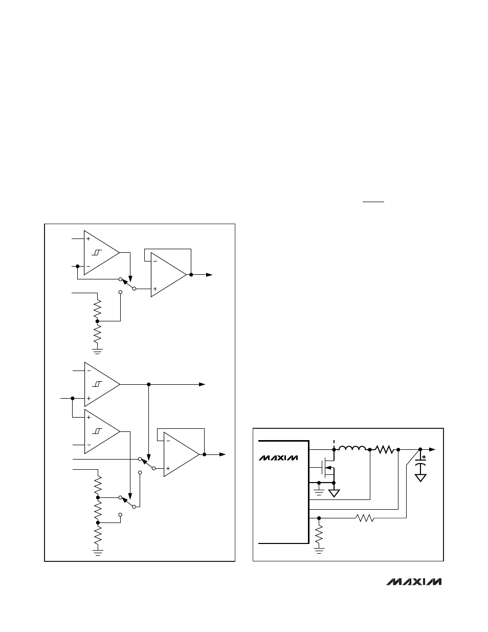
age changes apply to the combined output. Figure 9 is
the SMPS target decode block diagram.
Preset/Adjustable Output Voltages
(Dual-Mode Feedback)
Connect REFIN1 to V
CC
to set the SMPS1 voltage to
preset 1.05V. Connect FB2 to REF to set the SMPS2
voltage to preset 1.5V. The SMPS1 output voltage can
be adjusted up to 2V by changing REFIN1 voltage with-
out using an external resistive voltage-divider. The out-
put voltage of SMPS2 can be adjusted with an external
resistive voltage-divider between CSL2 and GND with
the center tap connected to FB2 (Figure 10). Choose
R
FB2LO
(resistance from FB2 to GND) to be approxi-
mately 10k
Ω and solve for R
FB2HI
(resistance from
CSL2 to FB2) using the equation:
The MAX17007A/MAX17008 regulate the valley of the
output ripple, so the actual DC output voltage is higher
than the slope compensated target by 50% of the out-
put ripple voltage. Under steady-state conditions, the
MAX17007A/MAX17008s’ internal integrator corrects for
this 50% output ripple voltage error, resulting in an out-
put-voltage accuracy that is dependent only on the off-
set voltage of the integrator amplifier provided in the
Electrical Characteristics
table.
Dynamic Output Voltages (REFIN1)
The MAX17007A/MAX17008 regulate the output to the
voltage set at REFIN1. By changing the voltage at
REFIN1 (Figure 11), the MAX17007A/MAX17008 can be
used in applications that require dynamic output volt-
age changes between two set points. For a step-volt-
age change at REFIN1, the rate of change of the output
voltage is limited either by the internal 9.5mV/μs slew-
rate circuit or by the component selection—inductor
current ramp, the total output capacitance, the current
limit, and the load during the transition—whichever is
slower. The total output capacitance determines how
much current is needed to change the output voltage,
while the inductor limits the current ramp rate.
R
R
V
V
FB HI
FB LO
CSL
2
2
2
0 7
1
=
⎛
⎝⎜
⎞
⎠⎟
.
-
Dual and Combinable QPWM Graphics
Core Controllers for Notebook Computers
24
______________________________________________________________________________________
V
CC
- 1V
FB2
REF - 0.3V
TARGET1
COMBINE
(FB2 = V
CC
)
PRESET
(FB1 = V
CC
)
PRESET
(FB2 = REF)
(B) SMPS2 TARGET DECODE
TARGET2
REF (2.0V)
0.7V
1.5V
5R
8R
7R
REFIN1
(A) SMPS1 TARGET DECODE
TARGET1
REF (2.0V)
1.05V
9.5R
10.5R
V
CC
- 1V
Figure 9. SMPS Target Decode Block Diagram
MAX17007A
MAX17008
DL2
GND
LX2
L2
FB2
CSL2
CSH2
R
FB2LO
C
OUT2
R
SENSE2
R
FB2HI
N
L2
Figure 10. Setting VOUT2 with a Resistive Voltage-Divider
