Table 1. uvlo state (v, Uvlo – Rainbow Electronics MAX16014 User Manual
Page 7

The MAX16013/MAX16014 can be configured as an
overvoltage switch controller to turn on/off a load (see
the Typical Application Circuit). When the programmed
overvoltage threshold is tripped, the internal fast com-
parator turns off the external p-channel MOSFET (P2),
pulling GATE2 to V
CC
to disconnect the power source
from the load. When the monitored voltage goes below
the adjusted overvoltage threshold, the MAX16013
enhances GATE2, reconnecting the load to the power
source (toggle ENABLE on the MAX16014 to reconnect
the load). The MAX16013 can be configured as an
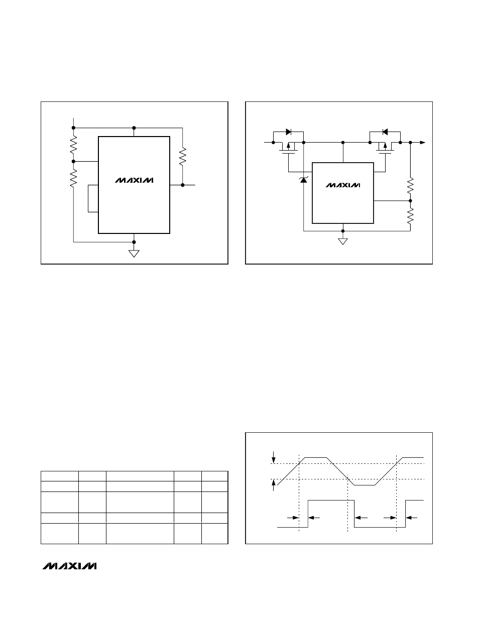
overvoltage limiter switch by connecting the resistive
divider to the load instead of V
CC
(Figure 3). See the
Overvoltage Limiter section.
Supply Voltage
Connect a 5.5V to 72V supply to V
CC
for proper opera-
tion. For noisy environments, bypass V
CC
to GND with a
0.1µF or greater capacitor. When V
CC
falls below the
UVLO voltage the following states are present (Table 1).
Hysteresis
Hysteresis adds noise immunity to the voltage monitors
and prevents oscillation due to repeated triggering
when the monitored voltage is near the threshold trip
voltage. The hysteresis in a comparator creates two trip
points: one for the rising input voltage (V
TH+
) and one
for the falling input voltage (V
TH-
). These thresholds are
shown in Figure 4.
Enable Inputs (EN or
EN
)
The MAX16011 offers an active-high enable input (EN),
while the MAX16010 offers both an active-high enable
input (EN) and active-low enable input (EN). For the
MAX16010, drive EN low or EN high to force the output
low. When the device is enabled (EN = high and EN =
low) the state of OUTA and OUTB depends on INA+
and INB- logic states.
MAX16010–MAX16014
Ultra-Small, Overvoltage Protection/
Detection Circuits
_______________________________________________________________________________________
7
MAX16012
IN+
REF
IN-
OUT
R
PULLUP
R1
R2
GND
V
BATT
V
CC
OUT
Figure 2. Typical Operating Circuit for the MAX16012
MAX16013
GATE1
SET
GATE2
V
CC
GND
P2
P1
R1
R2
V
BATT
Figure 3. Overvoltage Limiter Protection
Table 1. UVLO State (V
CC
< V
UVLO
)
PART
OUTA
OUTB
OUT
GATE2
MAX16010
Low
Low
—
—
MAX16011
Low
Low, LOGIC = low
High, LOGIC = high
—
—
MAX16012
—
—
Low
—
MAX16013
MAX16014
—
—
—
High
V
IN+
V
OUT
V
TH+
V
TH-
V
CC
0V
V
HYST
t
PROP
t
PROP
t
PROP
Figure 4. Input and Output Waveforms
