3 functional block diagram, 4 industry standard(s) compliance statement, 2 peripheral architecture – Texas Instruments TMS320DM644x User Manual
Page 9: 1 clock control, 2 signal descriptions, Statement, Architecture

www.ti.com
1.3
Functional Block Diagram
DIR
register
logic
Direction
register
SET_DATA
CLR_DATA
register
OUTDATA
register
GPIO
signal
Synchronizing flip−flops
INDATA
register
SET_RIS_TRIG
register
CLR_RIS_TRIG
register
SET_FAL_TRIG
register
CLR_FAL_TRIG
register
register
INSTAT
Edge
detection
logic
EDMA event
Interrupt
to ARM
or DSP
CPU
1.4
Industry Standard(s) Compliance Statement
2
Peripheral Architecture
2.1
Clock Control
2.2
Signal Descriptions
Peripheral Architecture
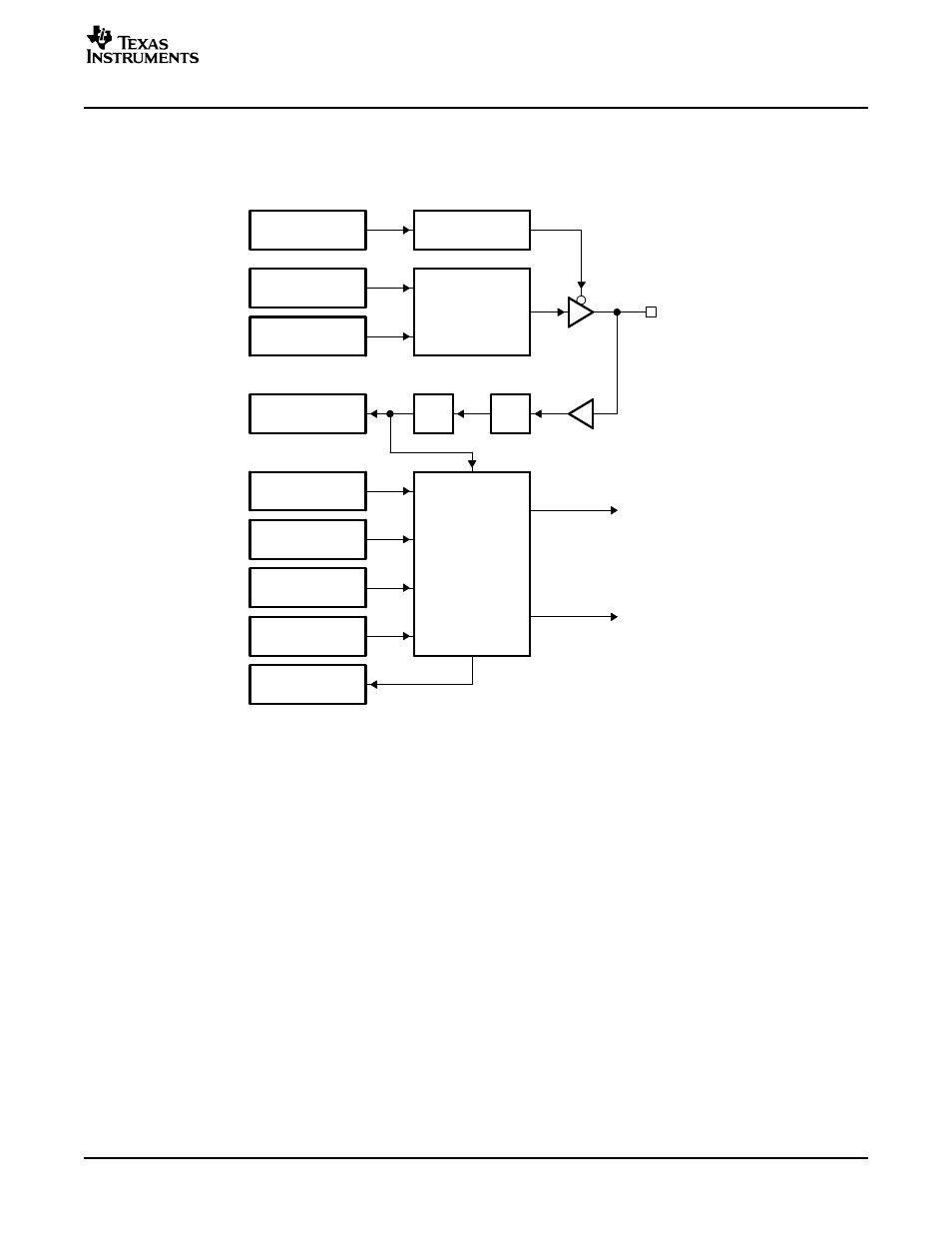
shows a block diagram of the GPIO peripheral.
Figure 1. GPIO Peripheral Block Diagram
The GPIO peripheral connects to external devices. While it is possible that the software implements some
standard connectivity protocol over GPIO, the GPIO peripheral itself is not compliant with any such
standards.
The following sections describe the GPIO peripheral.
The input clock to the GPIO peripheral is the SYSCLK5 chip-level clock. SYSCLK5 represents PLL1
divided by 6. The maximum operation speed for the GPIO peripheral is 10 MHz.
The DM644x device supports up to 71 GPIO signals. GPIO[53:0] are 1.8V I/O signals. GPIOV33_[16:0]
are 3.3V I/O signals. For information on the package pinout of each GPIO signal, refer to the device data
manual.
SPRUE25 – December 2005
General-Purpose Input/Output (GPIO)
9
