2 block diagram, 3 functional description, 2 block diagram 13.3 functional description – Lucent Technologies MN10285K User Manual
Page 297

I
2
C Bus Controller
Block Diagram
Panasonic Semiconductor Development Company
MN102H75K/F75K/85K/F85K LSI User Manual
296
Panasonic
13.2 Block Diagram
13.3 Functional Description
The I
2
C bus controller contains the registers shown in table 13-3. See the page
number indicated for register and bit descriptions.
■
Arbitration and bus busy control
The I
2
C bus controller allows software control, but implements communication
timing and bus arbitration completely in the hardware.
♦
Arbitration: Controlled by the software, but implemented completely
in the hardware.
♦
Bus busy: Checked by the hardware. This eliminates the need for the
software to check whether the bus is busy. The program can request a
transfer to the I
2
C bus at any time.
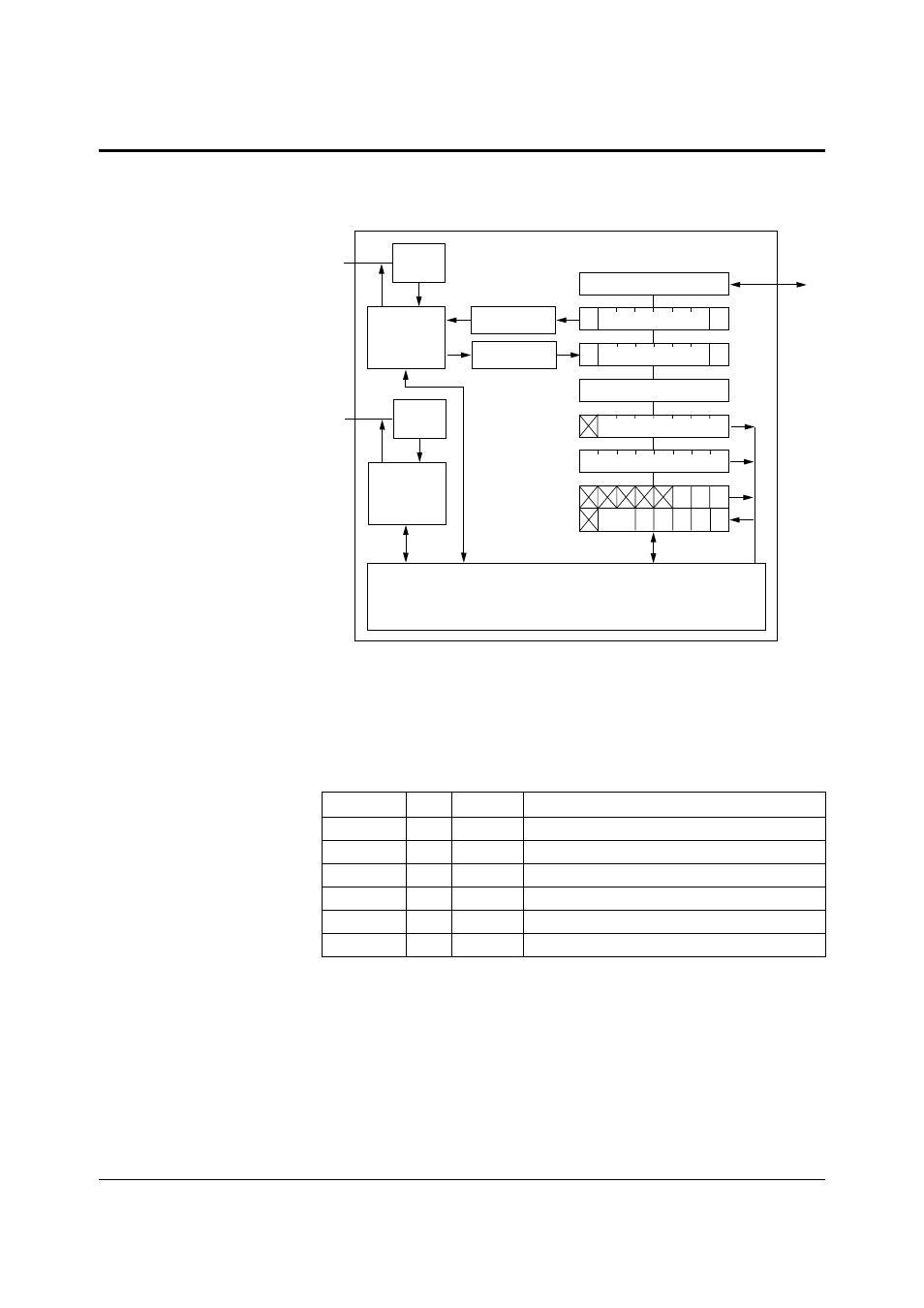
Figure 13-4 I
2
C Bus Controller Block Diagram
Table 13-3 Control Registers for Clamping Circuit
Register
Page
Address
Description
I2CDTRM
304
x’007E40’
I
2
C transmission data register
I2CDREC
305
x’007E42’
I
2
C reception data register
I2CMYAD
305
x’007E44’
I
2
C self address register
I2CCLK
306
x’007E46’
I
2
C clock control register
I2CBRST
306
x’007E48’
I
2
C bus reset register
I2CBSTS
306
x’007E4A’
I
2
C bus status register
SDA
Digital
filter
Data bus
controller
Parallel-to-serial
converter
Serial-to-parallel
converter
SCL
Digital
filter
Clock
controller
MSB
LSB
Transmission data register
MSB
LSB
Reception data register
Bus buffer
Address register
Clock register
ACK
BB
Address comparator
STO
LAB
STA
AAS
LRB
STS
MODE
Control register
Status register
I
2
C sequence controller
Register control
Bus busy logic
Arbitration logic
Clock prescaler
D[14 :0]
