Raster timing generator, Figure 2, Raster timing generator, input/output diagram – JVC Model 200 User Manual
Page 55
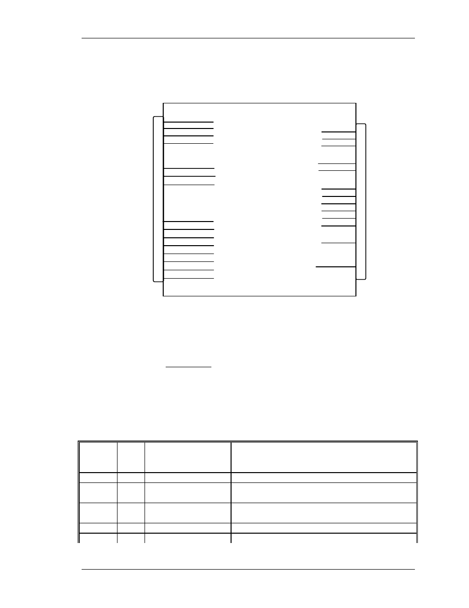
Chapter 2---System Description
Horizontal/Vertical Deflection Board uses these lines for proper
selection of retrace times.
B3 V_SYNC
B4 H_SYNC
B5 G_SYNC
HVPS_SYNC A14
A5 GRN_INPUT
A32 +5.1V
A31 +15V
B30 -15V
V_DRIVE B15
B19 ISYNC_CLK
B27 IIC_CLK
BLANKING B1
CLAMP B2
ODD_FIELD B23
SOURCE_VALID B24
280_CLK B21
B28 IIC_DATA
J13
J13
FROM
SCB
FROM
VPB
FROM
LVPS
TO
SCB
TO
VPB
RASTER
TIMING
GENERATOR
H_BAND1 B8
H_BAND0 B7
H_BAND2 B9
H_F2V B12
/H_ENABLE B11
H_DRIVE B16
TO
HVDB
TO
HVPS
B32 +5.1V
B31 +15V
A30 -15V
B29 GND
A29 +5.1V_STBY
TO
CDB
Figure 2
-
13. Raster Timing Generator, Input/Output Diagram
.
There are 9 LEDs on the RTG board (see Figure 5-2) that indicate
frequency bands, input modes and lock mode of the phase locked
loop.
IIC Interface
The RTG board uses the IIC bus interface for serial
communication with the System Controller Board. The information
transferred over the IIC bus is indicated below (I = input to RTG, O
= output from RTG). The RTG board does not use the interrupt
line of IIC bus interface:
Table 2-10. Raster Timing Generator IIC communication
Input /
Output
No.
of
bits
Information Description
I
1
FORCE_INTERNAL Selects internal syncs
I 1
TRI_LEVEL
Selects the tri level mode for the video clamp
signal (for HDTV)
I
1
SYNC_TIP
Selects the Sync tip option of video clamp
signal
I
1
VTR_MODE
Selects VTR mode of operation
I
9
Right blanking
Data for adjustment of right blanking
Model 200 Service Manual
2-41