Figure 2-5. high voltage power supply, i/o diagram, Table 2-1. high voltage power supply i/o signals, Raster timing generator pcb – JVC Model 200 User Manual
Page 25: J44 j45, High voltage power supply
Chapter 2---System Description
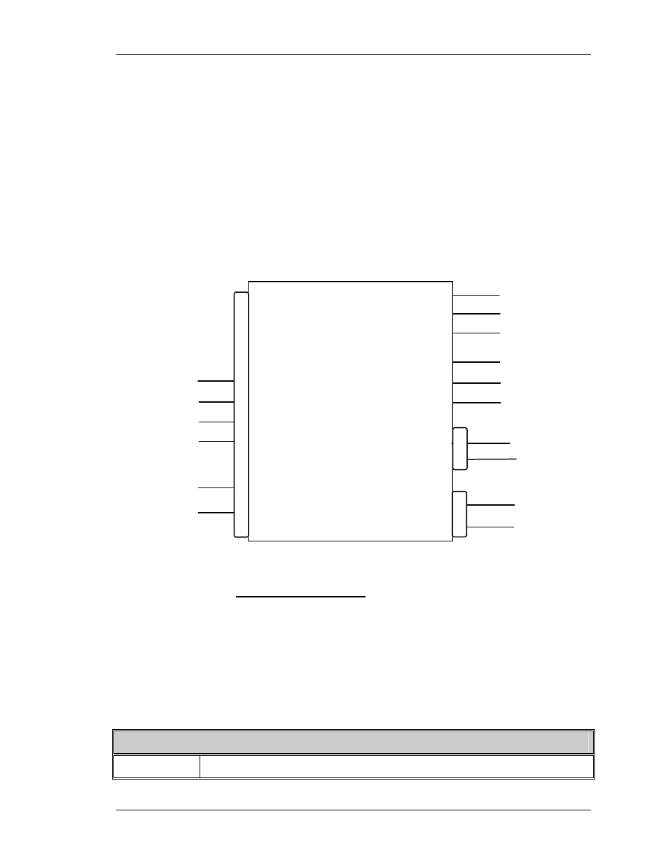
• Generation of focus voltage (G3) for all three CRTs (RGB)
• Generation of screen (G2 supply-Black Level) voltage for all
three CRTs
• Generation of G1 supply (Blanking) voltage
• Dynamic focus amplifier using H and V parabolas
• External ON/OFF and generation of /HV_OK signal
The High Voltage Power Supply I/O diagram (Figure 2-5) and the
list of inputs and outputs (Table 2-1), provide an understanding of
the operation of the HVPS to allow the technician to perform
module level troubleshooting.
AR C G N D
G 2 S UPP LY
G 1 S UPP LY
/H V O K
T
O
C
R
T
S
V I
A
V A B
R FO CU S J58-1
G FO CU S J59-1
B FO CU S J60-1
T
O
C R T
S
R AN O D E J58-1
G AN O D E J5 9-1
B AN O D E J60-1
T
O
C
R
T
S VI
A
V
A
B
H PA R A BO LA
F
R
O
M
C
D
BO
AR
D
V PA R A BO LA
+80V
F
R
O
M
LVPS
+15 V
-15
/H V E N A (/V A_O K)
H VP S_S YN C
FR
O
M
R
T
G
J45
5
11
J44
J45
1
3
14
8
9
10
12
6
13
(From VPB)
HIGH
VOLTAGE
POWER
SUPPLY
Figure 2-5. High Voltage Power Supply, I/O Diagram
The HVPS Input/Output
This section provides a comprehensive description of the inputs to
and outputs from the HVPS. The I/O descriptions are arranged by
the source/destination of the signal. The format used is such that
the assembly communicated with is used as the primary heading
of each output. Input refers to an input to the HVPS. Output refers
to an output from the HVPS. In each case the signals direction is
noted.
Table 2-1. High Voltage Power Supply I/O signals
Raster Timing Generator PCB
INPUT DESCRIPTION
Model 200 Service Manual
2-11