7 power measurement support, Power measurement support, Mobile intel – Intel 915GME User Manual
Page 30: 915gme express chipset voltage rails, Rv p
Mobile Intel
®
915GME Express Chipset —Theory of Operation
Mobile Intel
®
915GME Express Chipset
Development Kit User’s Manual
April 2007
30
Order Number: 317230-001US
For AC power loss, the system operation is defined by register settings in the Intel
ICH6-M. Upon the return of power, a BIOS option, set prior to the power loss, allows
the system to either go immediately to the S5 state, or reboot to the Full-On state, no
matter what the state was before the power loss. External logic for this functionality is
not necessary. If the BIOS remains in the S5 state after AC power loss, only the power
button or the RTC alarm can bring the system out of the S5 state. The status of enabled
wake events will be lost.
3.7
Power Measurement Support
Power measurement resistors are provided on the platform to measure the power of
most subsystems. All power measurement resistors have a tolerance of 1%. The value
of these power measurement resistors are 2 mΩ by default. Power on a particular
subsystem is calculated using the following formula:
R is the value of the sense resistor (typically 0.002 Ω)
V is the voltage measured across the sense resistor.
It is recommended that the user use a high precision digital multi-meter tool such as
the Agilent* 34401A digital multi-meter. Such a meter has 6½ digits of accuracy and
can provide a much greater accuracy in power measurement that a common 3½ digit
multimeter.
summarizes all the power measurement sense resistors located on the Mobile
Intel
®
915GME Express Chipset platform. All sense resistors are 0.002 Ω unless
otherwise noted.
R
V
P
2
=
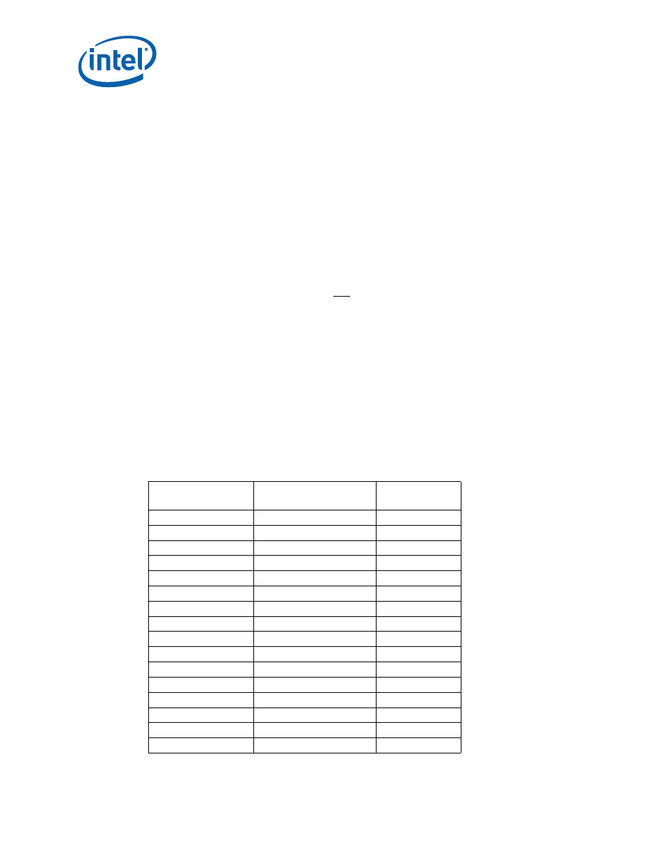
Table 6.
Mobile Intel
®
915GME Express Chipset Voltage Rails (Sheet 1 of 4)
Voltage Groups
Voltage Rail
Reference
Designator
1.0
+V1
U8A2.6
NC1-6_R
R8A3.2
1.5
+V1.5
Q3J2.1-3
+V1.5_VCCAUX
R7V1.1
1.5 Always
+V1.5A
R3J12.2
+V1.5A_ICH
R7V2.1
1.5 Switched
+V1.5S
Q3Y1.1-3
+V1.5S_DLVDS
R5U15.1
+V1.5S_DDRDLL
C5R3.1
+V1.5S_S_PCIE
C5T7.2
+V1.5S_3GPLL (0.5Ω)
R6R1.1
+V1.5S_MPLL
C4T1.1
+V1.5S_HPLL
C4R7.1
+V1.5S_DPLLA
C5T12.1
+V1.5S_DPLLB
C5T9.1
+V1.5S_HMPLL
R4D1.2