Maxim Integrated DS33R11 User Manual
General description, Applications, Functional diagram

DS33R11
Ethernet Mapper with Integrated
T1/E1/J1 Transceiver
www.maxim-ic.com
GENERAL DESCRIPTION
The DS33R11 extends a 10/100 Ethernet LAN
segment by encapsulating MAC frames in HDLC or
X.86 (LAPS) for transmission over a T1/E1/J1 data
stream.
The device performs store-and-forward of packets
with full wire-speed transport capability. The built-in
Committed Information Rate (CIR) Controller
provides fractional bandwidth allocation up to the line
rate in increments of 512kbps. The DS33R11 can
operate with an inexpensive external processor.
APPLICATIONS
Transparent LAN Service
LAN Extension
Ethernet Delivery Over T1/E1/J1
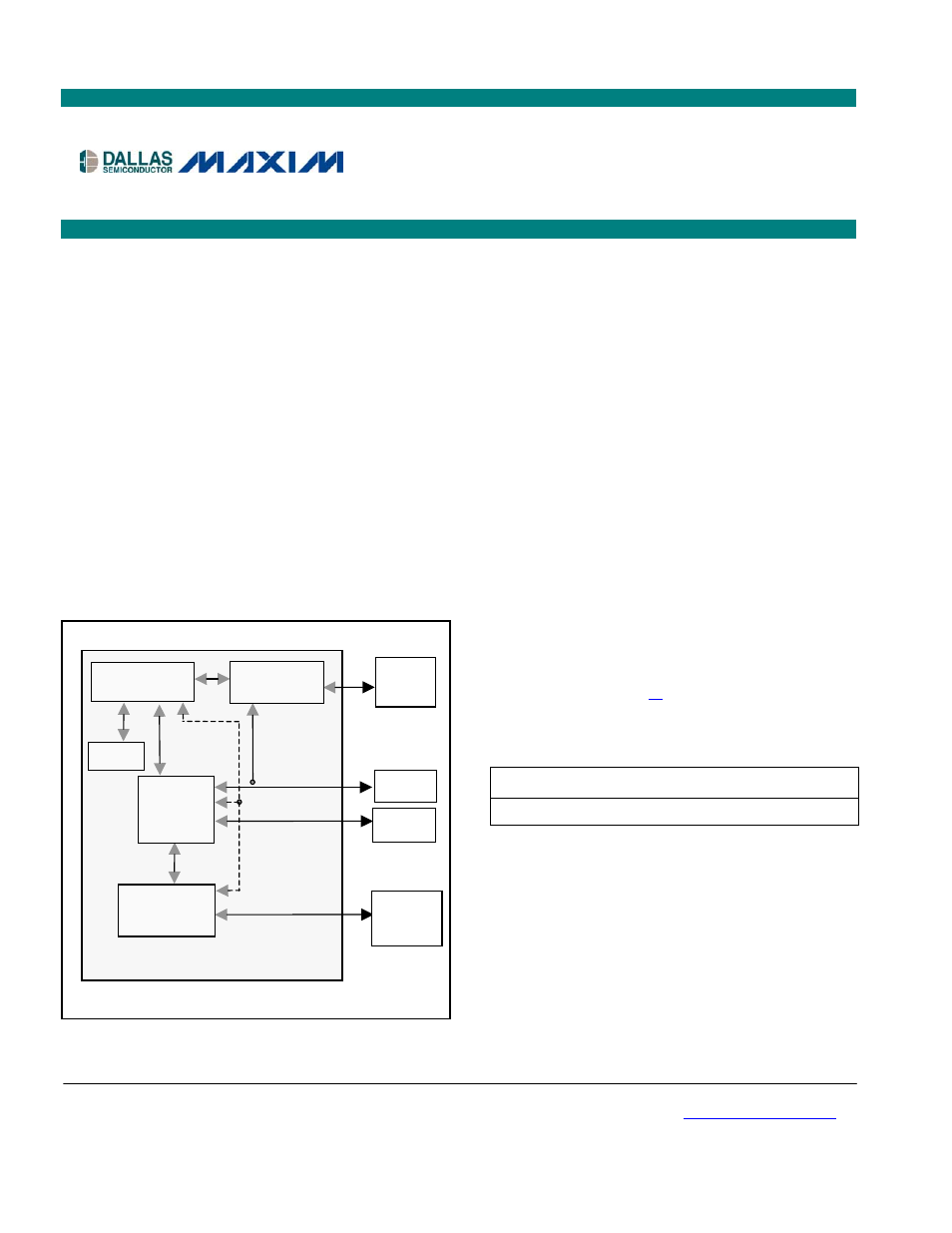
FUNCTIONAL DIAGRAM
FEATURES
10/100 IEEE 802.3 Ethernet MAC (MII and
RMII) Half/Full Duplex with Automatic Flow
Control
Integrated T1/E1/J1 Framer and LIU
HDLC/LAPS Encapsulation with
Programmable FCS and Interframe Fill
Committed Information Rate Controller
Provides Fractional Allocations in 512kbps
Increments
Programmable BERT for Serial (TDM)
Interface
External 16MB, 100MHz SDRAM Buffering
Parallel Microprocessor Interface
1.8V, 3.3V Supplies
Reference Design Routes on Two Signal
Layers
10/100
MAC
SDRAM
MII/RMII
μC
DS33R11
10/100
ETHERNET
PHY
SERIAL STREAM
T1/E1/J1
TRANSCEIVER
BERT
HDLC/X.86
MAPPER
T1/E1
LINE
IEEE 1149.1 JTAG Support
ORDERING INFORMATION
PART TEMP
RANGE
PIN-PACKAGE
DS33R11
-40°C to +85°C
256 BGA
1 of 344
REV:
030807
Note: Some revisions of this device may incorporate deviations from published specifications known as errata. Multiple revisions of any device
may be simultaneously available through various sales channels. For information about device errata, click here:
www.maxim-ic.com/errata
.
Document Outline
- TABLE OF CONTENTS
- 1 DESCRIPTION
- 2 FEATURE HIGHLIGHTS
- 2.1 General
- 2.2 Microprocessor Interface
- 2.3 HDLC Ethernet Mapping
- 2.4 X.86 (Link Access Protocol for SONET/SDH) Ethernet Mapping
- 2.5 Additional HDLC Controllers in the Integrated T1/E1/J1 Transceiver
- 2.6 Committed Information Rate (CIR) Controller
- 2.7 SDRAM Interface
- 2.8 MAC Interface
- 2.9 T1/E1/J1 Line Interface
- 2.10 Clock Synthesizer
- 2.11 Jitter Attenuator
- 2.12 T1/E1/J1 Framer
- 2.13 TDM Bus
- 2.14 Test and Diagnostics
- 2.15 Specifications Compliance
- 3 APPLICATIONS
- 4 ACRONYMS AND GLOSSARY
- 5 MAJOR OPERATING MODES
- 6 BLOCK DIAGRAMS
- 7 PIN DESCRIPTIONS
- 8 FUNCTIONAL DESCRIPTION
- 9 ETHERNET MAPPER
- 9.1 Ethernet Mapper Clocks
- 9.2 Resets and Low Power Modes
- 9.3 Initialization and Configuration
- 9.4 Global Resources
- 9.5 Per-Port Resources
- 9.6 Device Interrupts
- 9.7 Interrupt Information Registers
- 9.8 Status Registers
- 9.9 Information Registers
- 9.10 Serial Interface
- 9.11 Connections and Queues
- 9.12 Arbiter
- 9.13 Flow Control
- 9.14 Ethernet Interface Port
- 9.15 Ethernet MAC
- 9.16 BERT in the Ethernet Mapper
- 9.17 Transmit Packet Processor
- 9.18 Receive Packet Processor
- 9.19 X.86 Encoding and Decoding
- 9.20 Committed Information Rate Controller
- 10 INTEGRATED T1/E1/J1 TRANSCEIVER
- 10.1 T1/E1/J1 Clocks
- 10.2 Per-Channel Operation
- 10.3 T1/E1/J1 Transceiver Interrupts
- 10.4 T1 Framer/Formatter Control and Status
- 10.5 E1 Framer/Formatter Control and Status
- 10.6 Per-Channel Loopback
- 10.7 Error Counters
- 10.8 DS0 Monitoring Function
- 10.9 Signaling Operation
- 10.10 Per-Channel Idle Code Generation
- 10.11 Channel Blocking Registers
- 10.12 Elastic Stores Operation
- 10.13 G.706 Intermediate CRC-4 Updating (E1 Mode Only)
- 10.14 T1 Bit-Oriented Code (BOC) Controller
- 10.15 Additional (Sa) and International (Si) Bit Operation (E1 Only)
- 10.16 Additional HDLC Controllers in T1/E1/J1 Transceiver
- 10.17 Legacy FDL Support (T1 Mode)
- 10.18 D4/SLC-96 Operation
- 10.19 Programmable In-Band Loop Code Generation and Detection
- 10.20 Line Interface Unit (LIU)
- 10.21 MCLK Prescaler
- 10.22 Jitter Attenuator
- 10.23 CMI (Code Mark Inversion) Option
- 10.24 Recommended Circuits
- 10.25 T1/E1/J1 TRANSCEIVER BERT FUNCTION
- 10.27 Programmable Backplane Clock Synthesizer
- 10.28 Fractional T1/E1 Support
- 10.29 T1/E1/J1 Transmit Flow Diagrams
- 11 DEVICE REGISTERS
- 12 FUNCTIONAL TIMING
- 13 OPERATING PARAMETERS
- 13.1 Thermal Characteristics
- 13.2 MII Interface
- 13.3 RMII Interface
- 13.4 MDIO Interface
- 13.5 Transmit WAN Interface
- 13.6 Receive WAN Interface
- 13.7 SDRAM Timing
- 13.8 Microprocessor Bus AC Characteristics
- 13.9 AC Characteristics: Receive-Side
- 13.10 AC Characteristics: Backplane Clock Timing
- 13.11 AC Characteristics: Transmit Side
- 13.12 JTAG Interface Timing
- 14 JTAG INFORMATION
- 15 PACKAGE INFORMATION
- 16 DOCUMENT REVISION HISTORY
