Chapter 3: motherboard information, Block diagram, Chapter 3 – Lanner FW-7540 User Manual
Page 15: Motherboard information, Mb-7540 block diagram
10
Motherboard Information
Chapter 3
Network Application Platforms
Chapter 3:
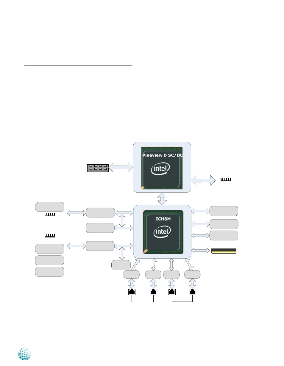
Motherboard Information
Block Diagram
The block diagram depicts the relationships among the
interfaces or modules on the motherboard. Please refer
to the following figure for your motherboard’s layout
design.
MB-7540 Block Diagram
X4 DMI
VG
A
Up to 4GB
MAX
Winbond
W83627
D
HG-
P
LPC
425 / 525
Processor
PC
I-E
x
1
USB
1x DDR3
800Mhz LONG-DIMM
2 x 6 pin Header
SATA
IDE
SPI
PCIE *1 over PCIE * 4
connector
(reserved for future use)
USB
2.0
PC
I-E
x1
USB 2.0
Mini PCI-E
CF II Socket
2 x SATA
SPI ROM
USB 2.0 front
USB pin Header
internal
PCI-E x1
Intel
82583V
PCI-E x1 PCI-E x1 PCI-E x1
Intel
82583V
Intel
82583V
Intel
82583V
1 pair Bypass
1 pair Bypass
Console Port using
RJ-45 connector
Console Pin
Header
KB/Mouse
Voltage Thermal
Sensor
TPM
(optional)
COM1
COM2
LPC Bus
(optional)
- LVC-2000 (39 pages)
- LVC-5000(N4) (42 pages)
- LVC-5550S (41 pages)
- LVC-5570 (48 pages)
- LVC-5770 (49 pages)
- FW-6432 (16 pages)
- FW-7525 (41 pages)
- FW-5330 (38 pages)
- FW-6486 (18 pages)
- FW-6436 (19 pages)
- FW-7573 (44 pages)
- FW-7568 (52 pages)
- FW-8759 (47 pages)
- FW-7581 (23 pages)
- FW-8758 (42 pages)
- FW-7610 (44 pages)
- FW-8756 (24 pages)
- FW-7575 (48 pages)
- FW-8760 (53 pages)
- FW-8877 (46 pages)
- FW-8892 (58 pages)
- FW-8893C (49 pages)
- FX-3411 (48 pages)
- FW-8894 (31 pages)
- FW-8771 (47 pages)
- RS12-38800 (64 pages)
- MR-320 (20 pages)
- FX-3210 (54 pages)
- MR-301 (16 pages)
- MR-350 (12 pages)
- MR-330A (16 pages)
- MR-730 (18 pages)
- VES-220 (19 pages)
- VES-270 (19 pages)
- VES-310 (15 pages)
- VES-310 V2 (20 pages)
- VES-500 (21 pages)
- EM-F345 (30 pages)
- VES-8X2 (16 pages)
- VES-8X6 (17 pages)
- LEC-2026 (67 pages)
- LEC-2010 (65 pages)
- LEC-2136 (20 pages)
- LEC-2050 (38 pages)