Sundance SMT702 User Manual
Page 54
0
The Voltage is coded on 10 bits.
4.3.1.2.37
Amount of samples stored in DDR2 – Bank A – 0x18C
(write).
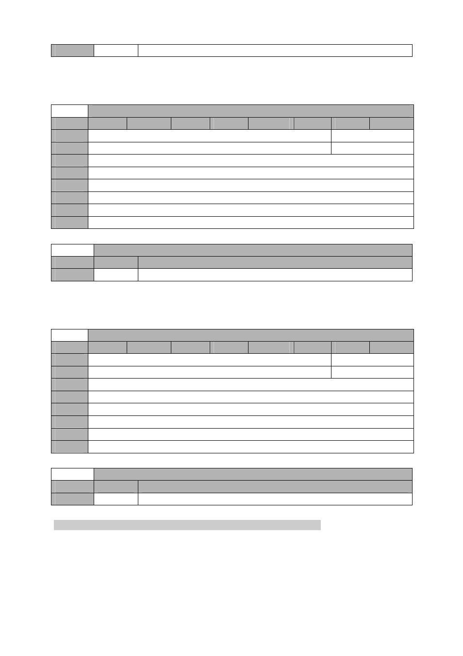
Offset 0x0400 –
Amount of samples stored in DDR2 – Bank A – 0x18C (read).
Byte
Bit 7
Bit 6
Bit 5
Bit 4
Bit 3
Bit 2
Bit 1
Bit 0
3
Reserved
Amount of samples
Default
‘000000’
‘00’
2
Amount of samples
Default
‘00000000’
1
Amount of samples
Default
‘00000000’
0
Amount of samples
Default
‘00000000’
Offset 0x0400 –
Amount of samples stored in DDR2 – Bank A – 0x18C (read).
Setting
Bit 25..0
Amount of samples.
0
Returns the amount of samples currently left to be transferred to the host.
4.3.1.2.38
Amount of samples stored in DDR2 – Bank B – 0x190
(write).
Offset 0x0400 –
Amount of samples stored in DDR2 – Bank B – 0x190 (read).
Byte
Bit 7
Bit 6
Bit 5
Bit 4
Bit 3
Bit 2
Bit 1
Bit 0
3
Reserved
Amount of samples
Default
‘000000’
‘00’
2
Amount of samples
Default
‘00000000’
1
Amount of samples
Default
‘00000000’
0
Amount of samples
Default
‘00000000’
Offset 0x0400 –
Amount of samples stored in DDR2 – Bank B – 0x190 (read).
Setting
Bit 25..0
Amount of samples.
0
Returns the amount of samples currently left to be transferred to the host.
4.3.2
System Monitor.
Virtex 5 FPGAs implement a function block called System Monitor (Xilinx). It allows
the user to monitor the FPGA Die temperature, the FPGA core voltage (Vccint) and
the Auxiliary voltage (Vccaux). It also provides the minimum and maximum values
measured since a system monitor reset has been applied.