Sundance SMT702 User Manual
Page 37
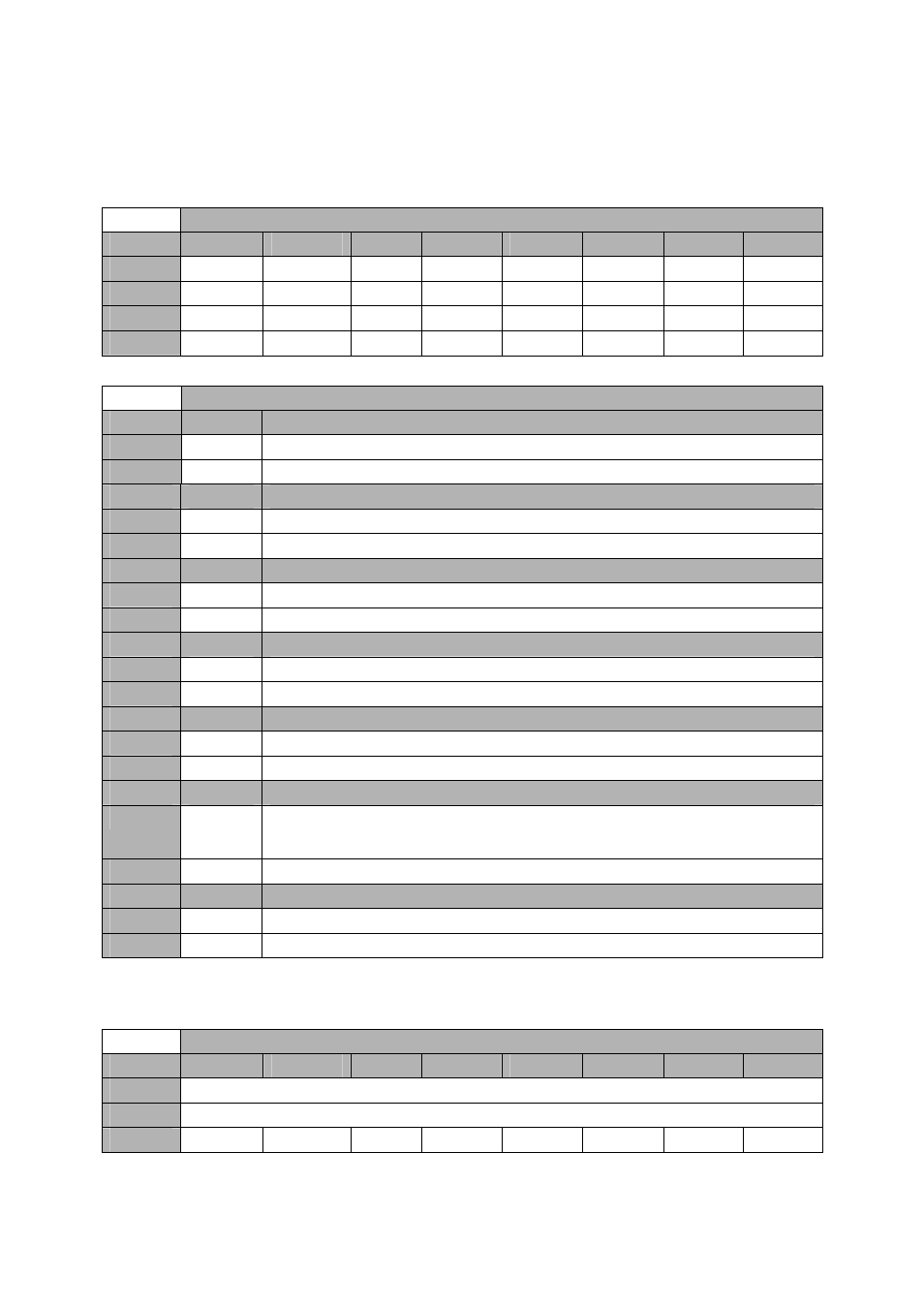
4.3.1.2.6
ADCA (ADC083000) Register 0x1 – Configuration
Register – 0x44 (write).
Offset 0x0400 -
ADCA (ADC083000) Register 0x1 – Configuration Register – 0x44 (write)
Byte
Bit 7
Bit 6
Bit 5
Bit 4
Bit 3
Bit 2
Bit 1
Bit 0
1
Reserved
DRE
RTD
DCS
DCP
nDE
OV
OE
Default
‘1’
‘1’
‘0’
‘1’
‘0’
‘1’
‘1’
‘0’
0
Reserved
Reserved
Reserved
Reserved
Reserved
Reserved
Reserved
Reserved
Default
‘1’
‘1’
‘1’
‘1’
‘1’
‘1’
‘1’
‘1’
Offset 0x0400 -
ADCA (ADC083000) Register 0x1 – Configuration Register – 0x44 (write)
Setting
Bit 14
Description (DRE – Differential Reset Enable)
0
0
Single-ended Reset enabled.
1
1
Differential Reset enabled.
Setting
Bit 13
Description (RTD – resistor Trim Disable)
0
0
Normal Operation.
1
1
Input termination resistor is not trimmed during calibration cycle.
Setting
Bit 12
Description (DCS – Duty Cycle Stabilizer)
0
0
Stabilisation circuit disabled.
1
1
Duty Cycle Stabilizer applied to the sampling clock.
Setting
Bit 11
Description (DCP – DDR Clock Phase – DDR Mode only)
0
0
0° phase – ADC output clock time-aligned with data.
1
1
90° phase – ADC output clock placed in the middle of data.
Setting
Bit 10
Description (nDE – DDR Enable)
0
0
DDR Mode.
1
1
SRD Mode.
Setting
Bit 9
Description (OV – LVDS Output Voltage amplitude)
0
0
Reduced output amplitude – 510mV. This setting is recommended on the SMT702. It
reduces the overall noise on the board and therefore increases the performance of the
ADCs.
1
1
Standard output amplitude – 710mV.
Setting
Bit 8
Description (OE –Output Edge)
0
0
1:4 Demux Mode (DDR Mode must be Selected).
1
1
1:2 Demux Mode (DDR Mode must be selected).
4.3.1.2.7
ADCA (ADC083000) Register 0x2 – Offset Adjust – 0x48
(write and read).
Offset 0x0400 -
ADCA (ADC083000) Register 0x2 – Offset Adjust – 0x48 (write and read)
Byte
Bit 7
Bit 6
Bit 5
Bit 4
Bit 3
Bit 2
Bit 1
Bit 0
1
Offset Value
Default
“00000000”
0
Reserved
Reserved
Reserved
Reserved
Reserved
Reserved
Reserved
Reserved